
CMOS 8-BIT SINGLE CHIP MICROCOMPUTER Product Manual


CHAPTER 5: SERIAL PROGRAMMING
6 EPSON S5U1C8F360Z1 MANUAL
(ADAPTER BOARD FOR S1C8F360/8F361)
CHAPTER 5SERIAL PROGRAMMING
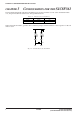
The S1C8F360 Adapter Board (S5U1C8F360Z1) connected to the On Board Programming Writer
(S5U1C88000W3) allows writing user data to the Flash EEPROM built into the S1C8F360/8F361 (package
model) placed on its IC socket using the On Board Programming Writer Control Software
(S5U1C8F360Y3).
Refer to "Appendix PROM programming" in the "S1C8F360 Technical Manual" for the programming
procedure.
5.1 Setting the Jumpers
Before performing serial programming, set the jumpers for the power unit as shown in Table 5.1.1.
Note: Be aware that the configuration is different between the S1C8F360 and the S1C8F361.
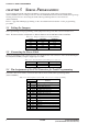
Table 5.1.1 Jumper settings for serial programming
Jumper
V
DD
V
SS
AV
DD
AV
SS
AV
REF
S1C8F360
short
short
short
short
short
S1C8F361
short
short
open
open
short
5.2 Connecting the Power Cable
Serial programming needs external power to be supplied to the CN5 connector on the S1C8F360 Adapter
Board (S5U1C8F360Z1) using the supplied power cable.
Table 5.2.1 Pin assignment of the CN5 power connector
CN5
1
2
Power cable
Red
Black
Power supply
V
DD
V
SS
5.3 Pin Assignment of the CN4 Connector for Serial Programming
The CN4 connector is used to connect the SIO cable from the On Board Programming Writer
(S5U1C88000W3).
Table 5.3.1 Pin assignment of the CN4 connector for serial programming
CN4
No.
1
2
3
4
5
6
7
8
9
10
11
12
13
14
15
16
Pin name
V
D1F
V
DD
CLKW
V
SS
SCLK
V
SS
TXD
V
SS
RXD
V
SS
RESET
V
SS
SPRG
V
SS
N.C.
N.C.
Function
Programming power supply pin
Power supply pin
System clock output pin
GND pin
Serial I/F clock output pin
GND pin
Serial I/F data output pin
GND pin
Serial I/F data input pin
GND pin
Initial reset output pin
GND pin
Programming mode setup output pin
GND pin