
Service manual


PhotoPC 3100Z Revision A
Operating Principles Circuit 44
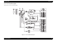
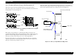
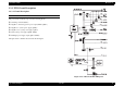
2.2.1.3 IC902 (H Driver) and IC904 (V Driver)
An H driver (IC902) and V driver (IC904) are necessary in order to generate the clocks
(vertical transfer clock, horizontal transfer clock and electronic shutter clock) which
drives the CCD.
IC902 is an inverter IC which drives the horizontal CCDs (H1 and H2). In addition the
XV1-XV4 signals which are output from IC102 are the vertical transfer clocks, and the
XSG1 and XSG signal which is output from IC102 is superimposed onto XV1 and
XV3 at IC904 in order to generate a ternary pulse. In addition, the XSUB signal which
is output from IC102 is used as the sweep pulse for the electronic shutter, and the RG
signal which is output from IC102 is the reset gate clock.
Figure 2-6. IC902/IC904 Block Diagram
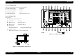
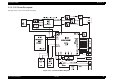
2.2.1.4 IC905 (CDS, AGC Circuit and A/D Converter)
The video signal which is output from the CCD is input to Pins (30) of IC905. There
are S/H blocks inside IC905 generated from the XSHP and XSHD pulses, and it is here
that CDS (correlated double sampling) is carried out.
After passing through the CDS circuit, the signal passes through the AGC amplifier. It
is A/C converted internally into a 12-bit signal, and is then input to IC102 of the CA2
circuit board. The gain of the AGC amplifier is controlled by pin (45)-(48) serial signal
which is output from IC102 of the CA2 board.
Figure 2-7. IC905 Block Diagram
IC902 IC904