MQ162-03 Application Manual Real Time Clock Module RTC-72421/72423 Model Product Number RTC-72421 A Q4272421x000100 RTC-72421 B Q4272421x000200 RTC-72423 A Q4272423x000600 RTC-72423 Q4272423x000700
In pursuit of "Saving" Technology ,Epson electronic device. Our Lineup of semiconductors, Liquid crystal displays and quartz devices assists in creating the products of our customers' dreams. Epson IS energy savings. NOTICE • The material is subject to change without notice. • Any part of this material may not be reproduced or duplicated in any form or any means without the written permission of Seiko Epson. • The information, applied circuit, program, using way etc.
RTC - 72421 / 72423 CONTENTS Overview ............................................................................................. 1 Block diagram ..................................................................................... 1 Terminal connections .......................................................................... 2 Terminal functions............................................................................... 3 Characteristics ...................................................
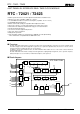
RTC - 72421 / 72423 4-BIT PARALLEL INTERFACE REAL TIME CLOCK MODULE RTC - 72421 / 72423 • Built-in crystal unit removes need for adjustment and reduces installation costs • Microprocessor bus compatible ( tWW, tRD = 120 ns ) • Use of C-MOS IC enables low current consumption ( 5 µA Max., at VDD = 2.
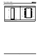
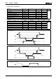
RTC - 72421 / 72423 Terminal connections RTC-72421 STD.P 1 CS0 ALE A0 2 3 4 RTC-72423 18 VDD 17 ( VDD ) 16 ( VDD ) 15 CS1 A1 5 14 D0 A2 6 13 D1 A3 7 12 D2 RD 8 11 D3 GND 9 10 WR STD.P 1 CS 0 2 24 N.C. 3 VDD 23 ( VDD ) 22 ( VDD ) ALE 4 21 N.C. A0 5 20 CS1 N.C. 6 19 D0 A1 7 18 N.C. N.C. 8 17 N.C. A2 9 16 D1 A3 10 15 D2 RD 11 14 D3 GND 12 13 WR The (VDD) pins are at the same electrical level as VDD. Do not connect these pins externally.
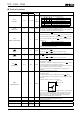
RTC - 72421 / 72423 Terminal functions Signal Input/ou Pin No. tput RTC-72421 RTC-72423 Function Connect these pines to a bi-directional data bus or CPU data bus. Use this bus to read to and write from the internal counter and registers.
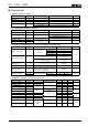
RTC - 72421 / 72423 Characteristics 1. Absolute maximum ratings Item Symbol Supply voltage Input voltage Output voltage VDD VI VO Storage temperature TSTG Condition Specification Ta=+25 °C Ta=+25 °C Ta=+25 °C RTC-72421 RTC-72423 −0.3 GND−0.3 GND−0.3 −55 −55 2. Recommended operating conditions Item Symbol Condition Supply voltage VDD Operating temperature TOPR Data hold voltage CS1 data hold time Operation recovery time VDH tCDR tr to to to to to Unit V V V °C °C 7.0 VDD+0.3 VDD+0.
RTC - 72421 / 72423 Switching characteristics (AC characteristics) 1. When ALE is used ( VDD=5 V ± 0.5 V, RTC-72421;Ta=−10 °C to +70 °C, RTC-72423;Ta=−40 °C to +85 °C ) Symbol Condition Min. Max.
RTC - 72421 / 72423 2. When ALE is fixed at VDD ( VDD=5 V ± 0.5 V, Symbol tSU(CS1) th(CS1) tSU(A-W) th(W-A) tw(W) tSU(D-W) th(W-D) trec(W) RTC-72421;Ta=−10 °C to +70 °C, RTC-72423;Ta=−40 °C to +85 °C ) Condition Min. Max. Unit 1000 1000 50 10 ns 120 80 10 200 ( VDD=5 V ± 0.
RTC - 72421 / 72423 Registers 1.
RTC - 72421 / 72423 4. Setting the fixed-period pulse output mode and fixed-period interrupt mode Mode Setting of fixed-period output timing ITRPT/STND STD.P pin Set low when active t1 bit 0 0 1 1 1 Set to 1 when active t0 bit 0 1 0 1 0 or 1 "0" Open-circuit Output period 1/64 s 1s 1 min. 1 hour MASK ITRPT/STND Fixed-period pulse output mode 0 0 Fixed-period interrupt mode 0 Fixed-period pulse output inhibited 1 5.
RTC - 72421 / 72423 Register description 1. Timing registers (1) S1 to Y10 registers These registers are 4-bit, positive logic registers in which the digits of the year, month, day, hour, minute, and second are continuously written in BCD code. For example, when(1, 0, 0, 1) has been written to the bits of the S1 register, the current value in the S1 register is 9. As described previously, data is handled by 4-bit BCD codes. Therefore, the S1 to Y10 registers consist of units registers and tens registers.
RTC - 72421 / 72423 2. CD register (control register D) (1) HOLD bit (D0) Use the HOLD bit when accessing the S1 and W registers. For details, see "Read/write of S1 to W registers". HOLD bit Function HOLD bit 0 The BUSY bit is always 1 (the BUSY status cannot be checked). 1 The BUSY status can be checked. When the HOLD bits is 1 and the BUSY bit is 0, read and write are enabled. When the HOLD bit is 1, any incrementation in the count is held within the RTC.
RTC - 72421 / 72423 *STD.P pin output IRQ FLAG bit 0 1 0 1 Interrupt generation (in synchronization with count incrementation) Writing of 0 IRQ FLAG bit. The output levels of the STD.P pin are low (down) and open circuit (up). Note: If the STD.P pin output remains low as set, subsequently generated interrupts are ignored. In order to prevent interrupts from being overlooked, write 0 to the IRQ FLAG bit before the next interrupt is generated, to return the STD.P pin to high. iii.
RTC - 72421 / 72423 2.Fixed-period interrupt mode (ITRPT/STND=1) MASK bit 0 IRQ FLAG bit 0 1 0 1 1 0 Nothing is output because the MASK bit is at 1 *STD. P pin Interrupt timing Reset at the point at which 0 is written to the IRF FLAG bit No interrupts are generated while the MASK bit is at 1 The output levels of the STD.P pin are low(down) and open circuit(up).
RTC - 72421 / 72423 4. CF register (control register F) (1) RESET bit (D0) Writing 1 to the RESET bit clears the sub-second bits of the internal counter down to the 1/256-seconds counter. The reset continues for as long as the RESET bit is 1. End the reset by writing 0 to the RESET bit. If the level of the CS1 pin goes low, the RESET bit is automatically cleared to 0. (2) STOP bit (D1) Writing 1 to the STOP bit stops the clock of the internal counter from the 1/8192 second bit onward.
RTC - 72421 / 72423 Using the RTC-72421/RTC-72423 1. Power-on procedure (initialization) When power is turned on, the contents of all registers and the output from the STD.P pin are undefined. Therefore, all the registers must be initialized after power on. Follow the procedure given below for initialization. Power On Start the counter Initialize the control registers (A) Check the status of the BUSY bit (B) STOP and RESET the counter (C) At ths point, there is no need to check the BUSY bit.
RTC - 72421 / 72423 (A)Starting the count START Set the CF register Reg.F ← 0*00B TEST ← 0 24/12 ← 0 or 1 STOP ← 0 RESET ← 0 Set the CE register This setting is not necessary when the STD.P pin is not used Set the CD register ← 0*00B 30 s ADJ ← 0 IRQ FLAG ← 0 or 1 ← 0 HOLD Reg.D Set the IRQ FLAG bit to 0 when fixed-period interrupt mode is used, or to 1when it is not used.
RTC - 72421 / 72423 2. Read/write of S1 to W registers Use one of the procedures shown below to access registers other than the control registers (CD, CE, and CF) while the RTC is operating. Note that the control registers can be accessed regardless of the status of the BUSY bit.
RTC - 72421 / 72423 4. Using the CS1 pin The RTC-72421/RTC-72423 has 2 chip-select signal systems: CS0 and CS1. Use CS0 as chip-select for ordinary bus access. CS1 is not only used for CPU bus control, it also has the main function of switching between standby mode and operating mode. (1) Functions Providing the CS1 pin with the rated voltage levels enables CS1 to have the following functions: • Enabling interface with microprocessor during operation within the operating voltage range (5.0 V ±0.
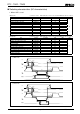
RTC - 72421 / 72423 Examples of connection to general-purpose microprocessor When connecting the RTC-72421/RTC-72423 to a microprocessor, carefully check the AC timings of both the RTC and the microprocessor. 1.
RTC - 72421 / 72423 External dimensions 1. RTC-72421 23.1 Max. 6.3 7.62 0.2 4.2 Min. Max. 1.52 0.46 0.25 2.54 Min. 2.54 0 - 15 2. RTC-72423 16.3 Max. 7.9 12.0 0.1 Min. 0.35 2.8 Max. 0.2 1.0 0 - 10 1.
RTC - 72421 / 72423 Reference data 1. Example of frequency and temperature characteristics θT = +25 °C Typ. α = -0.035 × 10⁻⁶ Typ. × 10-6 1. Frequency and temperature characteristics can be approximated using the following equations. ∆fT = α ( θT - θX )2 : Frequency deviation in any ∆fT temperature 2 α ( 1 / °C ) : Coefficient of secondary temperature -6 2 ( −0.035±0.
RTC - 72421 / 72423 Application notes 1. Notes on handling This module uses a C-MOS IC to realize low power consumption. handling. (1) Static electricity Carefully note the following cautions when While this module has built-in circuitry designed to protect it against electrostatic discharge, the chip could still be damaged by a large discharge of static electricity. Containers used for packing and transport should be constructed of conductive materials.
Application Manual Distributor AMERICA EPSON ELECTRONICS AMERICA, INC. HEADQUARTER Atlanta Office Boston Office Chicago Office El Segundo Office 150 River Oaks Parkway, San Jose, CA 95134, U.S.A. Phone: (1)800-228-3964 (Toll free) : (1)408-922-0200 (Main) Fax: (1)408-922-0238 http://www.eea.epson.com 3010 Royal Blvd. South, Ste. 170, Alpharetta, GA 30005, U.S.A. Phone: (1)877-332-0020 (Toll free) : (1)770-777-2078 (Main) Fax: (1)770-777-2637 301Edgewater Place, Ste. 120, Wakefield, MA 01880, U.S.A.