
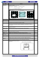
Technical information


http://w
w
w.epsontoyocom.co.jp
Glossary
GlossaryGlossary
Glossary
Epson Toyocom
Epson ToyocomEpson Toyocom
Epson Toyocom
Item Content Object
Start-up time
(t_str)
The time from power on until the wave form stabilizes.
However, voltage rise times depend on the power supply,
Therefore, the time depends on the power supply, and the time is measured from a specific set of initial
conditions.
OSC
Output enable(OE)
Output is switched to high impedance, and wired OR connection can be used to select multiple
outputs(freq ue nc y).
OE pin: High or open.
Specified frequency output = enabled.
OE pin: Low. Output is high impedance=disabled.
Oscillation is not stopped, so after the clock
is disabled, it is not synchronized with OE
(clock is co nti nuo us).
OSC
Outp ut freq ue nc y (f
o
)
The freque ncy o utput from the oscillator circuit or the crystal oscillator system. OSC
Output load conditions
The types and quantities (power) of the loads that can be connected to the oscillator.
Calculated for 1 TTL as l
OH
= -40 µA, l
OL
= 1.6 mA and for LS-TTL as I
OH
= -20 µA, l
OL
, = 0.4 mA.
OSC
Overtone
Vibration state when crystal is vibrating as a high harmonic(see base wavelength). It is harder
To matc h the overtone oscillation circuit with the c rystal unit than the fundamental oscillation circuit.
X’tal,OSC
Pass band
(BW)
Pass band (BW)
A band of frequencies B1 in which the attenuation is equal to or less than a specified value A1
A band of frequencies B1 in which the attenuation is equal to or less than the insertion loss L.
Stop band attenuation
Bands of frequencies B2 and B3 in which the attenuations are equal to or greater than specified values
A2 and A3 respectively.
Filter
Ripple (R) The difference between the max. and min. peak attenuation within a pass band. Filter
Recommended
drive level (DL)
Excitation level for optimum oscillation characteristics.
X’tal
Shunt capacitance(Co)
Charge capacitance between the two electrodes in the crystal unit.
X’tal
Soldering conditions
(T
SOL
)
Temperatures or times over these limits may result in characteristic degradation or destruction.
ALL
Stand-by (
ST
)
Function that halts crystal unit oscillation and frequency Division. Cuts the current consumed by the
oscillators circuit and the frequency division stage.
ST
pin-high or open: Specified frequency output.
ST
pin-low: Output is low level,oscillation stops.
: Output is low level (weak pull-down),
oscillation stops.
: Output is high impedance,
oscillation stops.
Please refer to each data sheet.
OSC
Shortage temperature
Range(T_stg)
Maximum absolute rating for the discharged state (no input of voltage, current or power).
Exposure to temperatures over this level may result in characteristic degradation or destruction.
To assure precision, store at room temperature whenever possible.
ALL
Spurious respo nse
A4 (dB)
Min. attenuation caused by extraordinary response in the stop band. Spurious response usually
appears at a higher frequency than the center frequency.
Filter
Supply voltage (V
CC
)
Voltage input to Vcc pin which will support continuous operation with specification characteristics.
OSC
Terminating impedance
(Zt)
Either of the impedances presented to the filter by the source or by the load.
(Rt: Resistive portion, Ct: Parallel capacitive portion including stray capacitance)
Filter
VSWR Voltage Standing Wave Ratio Filter
X'tal:Crystal Unit, OSC:Crystal Oscillator More details available on Epson Toyocom website.
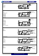
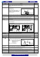
V
IH
V
IL
OE
Disabled
Enabled
High imped ance
t
PXZ
t
PZ X
OUTPUT
Timing
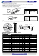
(MHz or kHz)
f
0
f
2
f
3
f
4
f
5
A3
A2
B3 B2
B1
R
L
D
f
1
f
6
f
7
f
8
(MHz or kHz)
(dB)
In the case that it defines with maximum loss in pass band.
f
0
+f
1
+f
2
+f
3
+f
4
A
4
A3
A2
B3 B2
B1
R
L
A1
D
-f
1
-f
5
-f
6
-f
7
(d B)
In t he case that it defin es with minimu m lo ss in pass band.
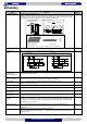
V
IH
V
IL
Stand-b
y
Low level
t
PXL
t
PLX
OUTPUT
Timing
V
OH
ST