MF595-04 CMOS 4-BIT SINGLE CHIP MICROCOMPUTER S1C62N82 Technical Manual S1C62N82 Technical Hardware/S1C62N82 Technical Software
NOTICE No part of this material may be reproduced or duplicated in any form or by any means without the written permission of Seiko Epson. Seiko Epson reserves the right to make changes to this material without notice.
PREFACE This part explains the function of the S1C62N82, the circuit configurations, and details the controlling method. II. S1C62N82 Technical Software This part explains the programming method of the S1C62N82. Software I. S1C62N82 Technical Hardware Hardware This manual is individualy described about the hardware and the software of the S1C62N82.
The information of the product number change Starting April 1, 2001, the product number will be changed as listed below. To order from April 1, 2001 please use the new product number. For further information, please contact Epson sales representative.
Hardware I.
CONTENTS CONTENTS CHAPTER 2 INTRODUCTION ............................................................... I-1 1.1 Configuration ................................................................... I-1 1.2 Features .......................................................................... I-2 1.3 Block Diagram ................................................................. I-4 1.4 Pin Layout Diagram ......................................................... I-5 1.5 Pin Description ................
CONTENTS CHAPTER 4 PERIPHERAL CIRCUITS AND OPERATION ...................... I-14 4.1 Memory Map .................................................................. I-14 4.2 Oscillation Circuit ............................................................ I-22 OSC1 oscillation circuit ........................................... OSC3 oscillation circuit ........................................... Configuration of oscillation circuit ........................... Control of oscillation circuit ...............
CONTENTS Stopwatch Timer ............................................................ I-58 Configuration of stopwatch timer ............................ Count-up pattern .................................................... Interrupt function ................................................... Control of stopwatch timer ...................................... 4.9 I-58 I-59 I-60 I-61 Supply Voltage Detection (SVD) Circuit and Heavy Load Protection Function .............................
CONTENTS CHAPTER 5 BASIC EXTERNAL WIRING DIAGRAM ........................... I-117 CHAPTER 6 ELECTRICAL CHARACTERISTICS ................................... I-121 6.1 Absolute Maximum Rating ............................................ I-121 6.2 Recommended Operating Conditions ........................... I-122 6.3 DC Characteristics ........................................................ I-123 6.4 Analog Circuit Characteristics and Power Current Consumption ..................................
CHAPTER 1: INTRODUCTION CHAPTER 1 INTRODUCTION Each member of the S1C62N82 Series of single chip microcomputers feature a 4-bit S1C6200A core CPU, 2,048 words of ROM (12 bits per word), 224 words of RAM (4 bits per word), an LCD driver, 5 bits for input ports (K00–K03 and K10), 7 bits for output ports (R00–R03 and R10–R12), one 4bit I/O port (P00–P03), two timer (clock timer and stopwatch timer), and a melody generator.
CHAPTER 1: INTRODUCTION 1.2 Features Built-in oscillation circuit Crystal or CR oscillation circuit (32.
CHAPTER 1: INTRODUCTION Interrupts: Input port interrupt External interrupt Timer interrupt Internal interrupt Melody interrupt Current consumption S1C62N82 ........ At S1C62N82 ........ At S1C62L82 ........ At S1C62L82 ........ At S1C62A82 ........ At Supply form 80-pin QFP (plastic) or chip S1C62N82 TECHNICAL HARDWARE 32 kHz 32 kHz 32 kHz 32 kHz 1 MHz EPSON 2 systems 2 systems 1 system 1.5 µA (Typ.) 4.0 µA (Typ.) 1.5 µA (Typ.) 4.0 µA (Typ.) 150 µA (Typ.
CHAPTER 1: INTRODUCTION ROM 2,048x12 OSC RESET OSC4 OSC3 OSC2 OSC1 1.3 Block Diagram System Reset Control Core CPU S1C6200A RAM 224x4 Interrupt Generator SEG0 COM7/SEG38 COM6/SEG39 COM5/SEG40 COM4/SEG41 LCD Driver I Port Test Port K00~K03 I/O Port P00~P03 K10 TEST COM0 VDD VL1 VL4 CA CD VS1 Vss CMPP CMPM Power Controller O Port Comparator & SVD R00~R03 R10, R11 Timer MO Stop Watch Melody R12 Fig. 1.3.
CHAPTER 1: INTRODUCTION 1.
CHAPTER 1: INTRODUCTION QFP14 60 41 61 40 Index 80 21 1 20 Pin No Pin Name Pin No Pin Name Pin No Pin Name Pin No Pin Name Pin No Pin Name I-6 1 SEG0 17 SEG16 33 K00 49 SEG30 65 CD 2 SEG1 18 SEG17 34 RESET 50 SEG31 66 CC 3 SEG2 19 SEG18 35 CMPP 51 SEG32 67 CB 4 SEG3 20 SEG19 36 CMPM 52 SEG33 68 CA 5 SEG4 21 R03 37 COM3 53 SEG34 69 V L4 6 SEG5 22 R02 38 COM2 54 SEG35 70 V L3 7 SEG6 23 R01 39 COM1 55 SEG36 71 V L2 8 SEG7 24 R
CHAPTER 1: INTRODUCTION 1.5 Pin Description Table 1.5.1 Pin description Terminal Name Pin No.
CHAPTER 2: POWER SUPPLY AND INITIAL RESET CHAPTER 2 POWER SUPPLY AND INITIAL RESET 2.1 Power Supply By externally providing a single power supply (*1) between VDD and VSS, the S1C62N82 Series produces the internally required voltage through the constant voltage circuit and voltage booster/reducer circuit. In S1C62N82/62A82, the constant voltage circuit produces VS1 voltage for oscillation and internal circuits, and VL2 voltage for LCD driving.
CHAPTER 2: POWER SUPPLY AND INITIAL RESET 2.2 Initial Reset To initialize the S1C62N82 Series circuits, an initial reset must be executed. There are three ways of doing this. (1) Initial reset by the oscillation detection circuit (2) External initial reset via the RESET pin (3) External initial reset by simultaneous high input to pins K00–K03 (depending on mask option) Figure 2.2.1 shows the configuration of the initial reset circuit.
CHAPTER 2: POWER SUPPLY AND INITIAL RESET Oscillation detection The oscillation detection circuit outputs the initial reset signal at power-on until the crystal oscillation circuit starts circuit oscillating, or when the crystal oscillation circuit stops oscillating for some reason. The circuit may malfunction if the power is turned on erroneously. In such cases, use one of the following two initial resetting methods.
CHAPTER 2: POWER SUPPLY AND INITIAL RESET Internal register following initialization An initial reset initializes the CPU as shown in the table below. Table 2.2.
CHAPTER 3: CPU, ROM, RAM CHAPTER 3 CPU, ROM, RAM 3.1 CPU The S1C62N82 Series employs the S1C6200A core CPU, so that register configuration, instructions, and so forth are virtually identical to those in other processors in the family using the S1C6200A. Refer to the "S1C6200/6200A Core CPU Manual" for details of the S1C6200A. Note the following points with regard to the S1C62N82 Series: (1) The SLEEP operation is not provided, so the SLP instruction cannot be used.
CHAPTER 3: CPU, ROM, RAM 3.2 ROM The built-in ROM, a mask ROM for the program, has a capacity of 2,048 × 12-bit steps. The program area is 8 pages (0–7), each consisting of 256 steps (00H–FFH). After an initial reset, the program start address is page 1, step 00H. The interrupt vector is allocated to page l, steps 02H– 0BH.
CHAPTER 4: PERIPHERAL CIRCUITS AND OPERATION (Memory Map) CHAPTER 4 PERIPHERAL CIRCUITS AND OPERATION Peripheral circuits (timer, I/O, and so on) of the S1C62N82 Series are memory mapped. Thus, all the peripheral circuits can be controlled by using memory operations to access the I/O memory. The following sections describe how the peripheral circuits operate. 4.
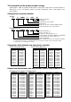
CHAPTER 4: PERIPHERAL CIRCUITS AND OPERATION (Memory Map) Table 4.1.
CHAPTER 4: PERIPHERAL CIRCUITS AND OPERATION (Memory Map) Table 4.1.
CHAPTER 4: PERIPHERAL CIRCUITS AND OPERATION (Memory Map) Table 4.1.
CHAPTER 4: PERIPHERAL CIRCUITS AND OPERATION (Memory Map) Table 4.1.
CHAPTER 4: PERIPHERAL CIRCUITS AND OPERATION (Memory Map) Table 4.1.
CHAPTER 4: PERIPHERAL CIRCUITS AND OPERATION (Memory Map) Table 4.1.
CHAPTER 4: PERIPHERAL CIRCUITS AND OPERATION (Memory Map) Table 4.1.
CHAPTER 4: PERIPHERAL CIRCUITS AND OPERATION (Oscillation Circuit) 4.2 Oscillation Circuit OSC1 oscillation circuit Crystal oscillation circuit The S1C62N82 Series has a built-in OSC1 crystal oscillation circuit (Typ. 32.768 kHz). As an external element, the OSC1 crystal oscillation circuit generates the operating clock for the CPU and peripheral circuitry by connecting the crystal oscillator (Typ. 32.768 kHz) and trimmer capacitor (5–25 pF). Figure 4.2.
CHAPTER 4: PERIPHERAL CIRCUITS AND OPERATION (Oscillation Circuit) OSC3 oscillation circuit In the S1C62N82 Series, the S1C62A82 has twin clock specification. The mask option enables selection of either the CR or ceramic oscillation circuit (OSC3 oscillation circuit) as the CPU's subclock.
CHAPTER 4: PERIPHERAL CIRCUITS AND OPERATION (Oscillation Circuit) Configuration of oscillation circuit The S1C62N82 and 62L82 have one oscillation circuit (OSC1), and the S1C62A82 has two oscillation circuits (OSC1 and OSC3). OSC1 is a crystal oscillation circuit or CR oscillation circuit (S1C62N82/62L82) that supplies the operating clock the CPU and peripheral circuits. OSC3 is either a CR or ceramic oscillation circuit.
CHAPTER 4: PERIPHERAL CIRCUITS AND OPERATION (Oscillation Circuit) Control of oscillation Table 4.2.1 lists the control bits and their addresses for the oscillation circuit. circuit Table 4.2.
CHAPTER 4: PERIPHERAL CIRCUITS AND OPERATION (Oscillation Circuit) I-26 Note - It takes at least 5 ms from the time the OSC3 oscillation circuit goes ON until the oscillation stabilizes. Consequently, when switching the CPU operation clock from OSC1 to OSC3, do this after a minimum of 5 ms have elapsed since the OSC3 oscillation went ON.
CHAPTER 4: PERIPHERAL CIRCUITS AND OPERATION (Input Ports) 4.3 Input Ports (K00–K03, K10) Configuration of input ports The S1C62N82 Series have a general-purpose input (4 bits + 1 bit). Each of the input port pins (K00–K03, K10) has an internal pull-down resistance. The pull-down resistance can be selected for each bit with the mask option. Figure 4.3.1 shows the configuration of input port. Interrupt request Kxx Data bus V DD Address V SS Fig. 4.3.
CHAPTER 4: PERIPHERAL CIRCUITS AND OPERATION (Input Ports) Input comparison registers and interrupt function All five input port bits (K00–K03, K10) provide the interrupt function. The conditions for issuing an interrupt can be set by the software for the five bits. Also, whether to mask the interrupt function can be selected individually for all five bits by the software. Figure 4.3.2 shows the configuration of K00–K03 and K10.
CHAPTER 4: PERIPHERAL CIRCUITS AND OPERATION (Input Ports) Interrupt mask registers Input comparison registers EIK03 EIK02 EIK01 EIK00 KCP03 KCP02 KCP01 KCP00 1 1 1 0 1 0 1 0 With the above setting, an interrupt for K00–K03 occurs under the following conditions. Input ports (1) K03 K02 K01 K00 1 0 1 0 (Initial value) ↓ (2) K03 K02 K01 K00 1 0 1 1 ↓ (3) K03 K02 K01 K00 0 0 1 1 ↓ (4) K03 K02 K01 K00 0 1 1 1 K03 K02 K01 K00 1 0 1 1 ↓ Fig. 4.3.
CHAPTER 4: PERIPHERAL CIRCUITS AND OPERATION (Input Ports) Input interrupt programing related precautions Port K input Active status Input comparison register Falling edge interrupt Active status Rising edge interrupt Mask register ➀ Fig. 4.3.4 Input interrupt timing Factor flag set Not set ➁ Factor flag set When the content of the mask register is rewritten, while the port K input is in the active status.
CHAPTER 4: PERIPHERAL CIRCUITS AND OPERATION (Input Ports) In addition, when the mask register = 1 and the content of the input comparison register is rewritten in the input terminal active status, an input interrupt factor flag may be set. Thus, you should rewrite the content of the input comparison register in the mask register = 0 status.
CHAPTER 4: PERIPHERAL CIRCUITS AND OPERATION (Input Ports) Control of input ports Tables 4.3.1 (a) and 4.3.1 (b) list the input port control bits and their addresses. Table 4.3.
CHAPTER 4: PERIPHERAL CIRCUITS AND OPERATION (Input Ports) Table 4.3.
CHAPTER 4: PERIPHERAL CIRCUITS AND OPERATION (Input Ports) KCP00–KCP03, KCP10 Input comparison registers (0E5H, 0E6H D0) The interrupt conditions for pins K00–K03 and K10 can be set with these registers. When 1 is read: When 0 is read: Reading: Falling edge Rising edge Valid Of the five bits of the input ports, the interrupt conditions can be set for the rising or falling edge of the input for each of the five bits (K00–K03 and K10) through the input comparison registers (KCP00–KCP03 and KCP10).
CHAPTER 4: PERIPHERAL CIRCUITS AND OPERATION (Input Ports) Reading of interrupt factor flags is available at EI, but be careful in the following cases. If the interrupt mask register value corresponding to the interrupt factor flags to be read is set to 1, an interrupt request will be generated by the interrupt factor flags set timing, or an interrupt request will not be generated. Be very careful when interrupt factor flags are in the same address. After an initial reset, these flags are set to 0.
CHAPTER 4: PERIPHERAL CIRCUITS AND OPERATION (Output Ports) 4.4 Output Ports (R00–R03, R10–R12) Configuration of output ports The S1C62N82 Series have 7 bits for general output ports (R00–R03 and R10–R12). Output specifications of the output ports can be selected individually with the mask option. Two kinds of output specifications are available: complementary output, and Pch open drain output. Also, the mask option enables the output ports R10 and R12 to be used as special output ports. Figure 4.4.
CHAPTER 4: PERIPHERAL CIRCUITS AND OPERATION (Output Ports) The mask option enables the following output port selection. Mask option (1) Output specifications of output ports The output specifications for the output ports (R00–R03, R10–R12) may be either complementary output or Pch open drain output for each of the seven bits. However, even when Pch open drain output is selected, a voltage exceeding the source voltage must not be applied to the output port.
CHAPTER 4: PERIPHERAL CIRCUITS AND OPERATION (Output Ports) FOUT (R10) When output port R10 is set for FOUT output, it outputs the clock of fosc3 and fosc1 or the divided fosc1. The clock frequency is selectable by mask option from the frequencies listed in Table 4.4.2. Table 4.4.2 FOUT clock frequency Setting Value fosc3 Clock Frequency (Hz) 1,000,000 (Typ.
CHAPTER 4: PERIPHERAL CIRCUITS AND OPERATION (Output Ports) Table 4.4.3 lists the output port control bits and their addresses. Control of output ports Table 4.4.
CHAPTER 4: PERIPHERAL CIRCUITS AND OPERATION (Output Ports) R12 (when MO or ENV is Special output port data (0F4H D2) selected) This bit will not affect the melody (MO) or envelope (ENV) signal at Rl2. R12 register is a general purpose register which can be read and written. When 1 is written: When 0 is written: Reading: No effect at R12 No effect at R12 Valid R10 (when FOUT is Special output port data (0F4H D0) selected) Controls the FOUT (clock) output.
CHAPTER 4: PERIPHERAL CIRCUITS AND OPERATION (I/O Ports) 4.5 I/O Ports (P00–P03) The S1C62N82 Series have a 4-bit general-purpose I/O port. Figure 4.5.1 shows the configuration of the I/O port. The four bits of the I/O port P00–P03 can be set to either input mode or output mode. The mode can be set by writing data to the I/O control register (IOC). Data bus Configuration of I/O port Input control Register Pxx Address Fig. 4.5.
CHAPTER 4: PERIPHERAL CIRCUITS AND OPERATION (I/O Ports) Mask option The output specification during output mode (IOC = 1) of the I/O port can be set with the mask option for either complementary output or Pch open drain output. This setting can be performed for each bit of the I/O port. However, when Pch open drain output has been selected, voltage in excess of the supply voltage must not be applied to the port. Control of I/O port Table 4.5.1 lists the I/O port control bits and their addresses.
CHAPTER 4: PERIPHERAL CIRCUITS AND OPERATION (I/O Ports) • When reading data When 1 is read: When 0 is read: High level Low level The pin voltage level of the I/O port is read. When the I/ O port is in the input mode the voltage level being input to the port pin can be read; in the output mode the output voltage level can be read. When the pin voltage is high (VDD) the port data read is 1, and when the pin voltage is low (VSS) the data is 0.
CHAPTER 4: PERIPHERAL CIRCUITS AND OPERATION (I/O Ports) IOC I/O control register (0FCH D0) The input or output I/O port mode can be set with this register. When 1 is written: When 0 is written: Reading: Output mode Input mode Valid The input or output mode of the I/O port is set in units of four bits. For instance, IOC sets the mode for P00–P03. Writing 1 to the I/O control register makes the I/O port enter the output mode, and writing 0, the input mode.
CHAPTER 4: PERIPHERAL CIRCUITS AND OPERATION (LCD Driver) 4.6 LCD Driver Configuration of LCD In the S1C62N82 Series, when selecting 1/8 duty, there are 8 common terminals (COM0–COM7) and 38 segment termidriver nals (SEG0–SEG37) available which allow up to 304 (i.e., 38 × 8) LCD segments to be driven. During selection of 1/4 duty, there are 4 common terminals (COM0–COM3) and 42 segment terminals (SEG0–SEG41) available which allow up to 168 (i.e., 42 × 4) LCD segments to be driven.
CHAPTER 4: PERIPHERAL CIRCUITS AND OPERATION (LCD Driver) COM0 -V DD -V L1 -V L2 -V L3 COM1 LCD lighting status COM0 COM1 COM2 COM3 SEG0–41 COM2 Not lit Lit COM3 -V DD -V L1 -V L2 -V L3 SEG 0–41 Fig. 4.6.
CHAPTER 4: PERIPHERAL CIRCUITS AND OPERATION (LCD Driver) 0 1 2 3 4 5 6 7 0 1 2 3 4 5 6 7 VDD VL1 VL2 COM0 VL3 VL4 VDD VL1 LCD lighting status COM0 COM1 COM2 COM3 COM4 COM5 COM6 COM7 SEG0–37 VL2 COM1 VL3 VL4 Not lit Lit VDD VL1 VL2 COM2 VL3 VL4 VDD VL1 VL2 VL3 VL4 VDD VL1 VL2 VL3 VL4 VDD SEG0–37 VL1 VL2 VL3 VL4 VDD VL1 VL2 VL3 VL4 Fig. 4.6.
CHAPTER 4: PERIPHERAL CIRCUITS AND OPERATION (LCD Driver) Switching between dynamic and static drive The S1C62N82 Series members allow software setting of the LCD static drive. This function enables easy adjustment (cadence adjustment) of the oscillation frequency of the OSC circuit. The procedure for executing of the LCD static drive is as follows: ➀ Write 1 to the CSDC register at address 0FBH D3. ➁ Write the same value to all registers corresponding to COM0–COM7 of the display memory.
CHAPTER 4: PERIPHERAL CIRCUITS AND OPERATION (LCD Driver) (1) Segment allocation Mask option (segment allocation) As shown in Figure 4.l.1, the S1C62N82 Series display data is decided by the display data written to the display memory (write-only) at address 090H–0DFH. The address and bits of the display memory can be made to correspond to the segment pins (SEG0–SEG41) in any combination through mask option.
CHAPTER 4: PERIPHERAL CIRCUITS AND OPERATION (LCD Driver) (2) Drive duty According to the mask option, either 1/4 or 1/8 duty can be selected as the LCD drive duty. Table 4.6.1 shows the differences in the number of segments according to the selected duty. Table 4.6.
CHAPTER 4: PERIPHERAL CIRCUITS AND OPERATION (LCD Driver) Table 4.6.2 shows the control bits of the LCD driver and their addresses. Figure 4.6.6 shows the display memory map. Control of LCD driver Table 4.6.
CHAPTER 4: PERIPHERAL CIRCUITS AND OPERATION (LCD Driver) CSDC LCD drive switch (0FBH D3) The LCD drive format can be selected with this switch. When 1 is written: When 0 is written: Reading: Static drive Dynamic drive Valid After an initial reset, dynamic drive (CSDC = 0) is selected. Display memory (090H–0DFH) The LCD segments are turned on or off according to this data.
CHAPTER 4: PERIPHERAL CIRCUITS AND OPERATION (Clock Timer) 4.7 Clock Timer Configuration of clock timer The S1C62N82 Series have a built-in clock timer driven by the source oscillator. The clock timer is configured as a seven-bit binary counter that serves as a frequency divider taking a 256 Hz source clock from a prescaler. The four high-order bits (16 Hz–2 Hz) can be read by the software. Figure 4.7.1 is the block diagram of the clock timer.
CHAPTER 4: PERIPHERAL CIRCUITS AND OPERATION (Clock Timer) Interrupt function Address 0E4H The clock timer can interrupt on the falling edge of the 32 Hz, 8 Hz, and 2 Hz signals. The software can mask any of these interrupt signals. Figure 4.7.2 is the timing chart of the clock timer. Register Frequency bits D0 16 Hz D1 8 Hz D2 4 Hz D3 2 Hz Clock timer timing chart Occurrence of 32 Hz interrupt request Occurrence of 8 Hz interrupt request Occurrence of 2 Hz interrupt request Fig. 4.7.
CHAPTER 4: PERIPHERAL CIRCUITS AND OPERATION (Clock Timer) Table 4.7.1 shows the clock timer control bits and their addresses. Control of clock timer Table 4.7.
CHAPTER 4: PERIPHERAL CIRCUITS AND OPERATION (Clock Timer) TM0–TM3 Timer data (0E4H) The 16 Hz to 2 Hz timer data of the clock timer can be read from this register. These four bits are read-only, and write operations are invalid. After an initial reset, the timer data is initialized to 0H. EIT32, EIT8, EIT2 Interrupt mask registers (0EBH D0–D2) These registers are used to mask the clock timer interrupt.
CHAPTER 4: PERIPHERAL CIRCUITS AND OPERATION (Clock Timer) TMRST Clock timer reset (0F9H D2) This bit resets the clock timer. When 1 is written: Clock timer reset When 0 is written: No operation Reading: Always 0 The clock timer is reset by writing 1 to TMRST. The clock timer starts immediately after this. No operation results when 0 is written to TMRST. This bit is write-only, and so is always 0 when read.
CHAPTER 4: PERIPHERAL CIRCUITS AND OPERATION (Stopwatch Timer) 4.8 Stopwatch Timer Configuration of stopwatch timer The S1C62N82 Series incorporate a 1/100 sec and 1/10 sec stopwatch timer. The stopwatch timer is configured as a two-stage, four-bit BCD timer serving as the clock source for an approximately 100 Hz signal (obtained by approximately dividing the 256 Hz signal output from the prescaler). Data can be read out four bits at a time by the software. Figure 4.8.
CHAPTER 4: PERIPHERAL CIRCUITS AND OPERATION (Stopwatch Timer) The stopwatch timer is configured as two four-bit BCD timers, SWL and SWH. The SWL timer, at the stage preceding the stopwatch timer, has an approximate 100 Hz signal as its input clock. It counts up every 1/100 sec and generates an approximate 10 Hz signal. The SWH timer has an approximate 10 Hz signal generated by the SWL timer for its input clock. It counts up every 1/10 sec and generates a 1 Hz signal. Figure 4.8.
CHAPTER 4: PERIPHERAL CIRCUITS AND OPERATION (Stopwatch Timer) The 10 Hz (approximate 10 Hz) and 1 Hz interrupts can be generated by the overflow of the SWL and SWH stopwatch timers, respectively. Also, software can separately mask the frequencies as described earlier. Figure 4.8.3 is the timing chart for the stopwatch timer.
CHAPTER 4: PERIPHERAL CIRCUITS AND OPERATION (Stopwatch Timer) Control of stopwatch Table 4.8.1 shows the stopwatch timer control bits and their addresses. timer Table 4.8.
CHAPTER 4: PERIPHERAL CIRCUITS AND OPERATION (Stopwatch Timer) SWL0–SWL3 1/100 sec stopwatch timer (0E2H) Data (BCD) of the 1/100 sec column of the stopwatch timer can be read. These four bits are read-only, and cannot be written to. After an initial reset, the timer data is set to 0H. SWH0–SWH3 1/10 sec stopwatch timer (0E3H) Data (BCD) of the 1/10 sec column of the stopwatch timer can be read. These four bits are read-only, and cannot be written to. After an initial reset, the timer data is set to 0H.
CHAPTER 4: PERIPHERAL CIRCUITS AND OPERATION (Stopwatch Timer) Reading of interrupt factor flags is available at EI, but be careful in the following cases. If the interrupt mask register value corresponding to the interrupt factor flags to be read is set to 1, an interrupt request will be generated by the interrupt factor flags set timing, or an interrupt request will not be generated. Be very careful when interrupt factor flags are in the same address. After an initial reset, these flags are set to 0.
CHAPTER 4: PERIPHERAL CIRCUITS AND OPERATION (SVD Circuit and Heavy Load Protection Function) 4.9 Supply Voltage Detection (SVD) Circuit and Heavy Load Protection Function Configuration of SVD circuit and heavy load protection function The S1C62N82 Series have a built-in supply voltage detection (SVD) circuit and a heavy load protection function. Figure 4.9.1 shows the configuration of the circuit.
CHAPTER 4: PERIPHERAL CIRCUITS AND OPERATION (SVD Circuit and Heavy Load Protection Function) If the source voltage is reduced by a heavy load while in the heavy load protection mode, the rate of decrease can be detected by hardware. After this, the heavy load is lost and even when the heavy load protection mode is released by software, the mode continues until the source voltage exceeds the voltage detected by the SVD circuit.
CHAPTER 4: PERIPHERAL CIRCUITS AND OPERATION (SVD Circuit and Heavy Load Protection Function) Operation of SVD detection timing The following explains the timing when the SVD circuit writes the result of supply voltage detection to the SVDDT register. The result of supply voltage detection is written to the SVDDT register by the SVD circuit, and this data can be read by the software to determine the supply voltage. There are two methods, explained below, for executing the detection by the SVD circuit.
CHAPTER 4: PERIPHERAL CIRCUITS AND OPERATION (SVD Circuit and Heavy Load Protection Function) Notice that even if the SVD circuit detects a drop in the supply voltage (1.2 V/2.4 V or less) and invokes the heavy load protection mode, this will be the same as when the software invokes the heavy load protection mode, in that the SVD circuit will be sampled with a timing synchronized to the 2 Hz output from the prescaler.
CHAPTER 4: PERIPHERAL CIRCUITS AND OPERATION (SVD Circuit and Heavy Load Protection Function) Control of SVD circuit and heavy load protection function Table 4.9.1 shows the control bits and their addresses for the SVD circuit and the heavy load protection function. Table 4.9.
CHAPTER 4: PERIPHERAL CIRCUITS AND OPERATION (SVD Circuit and Heavy Load Protection Function) SVDON SVD control on/off (0FAH D0) When 0 is written: SVD detection off When 1 is written: SVD detection on Reading: Valid When this bit is written, the SVD detection on/off operation is controlled. Large current is drawn during SVD detection, so keep SVD detection off except when necessary. When SVDON is set to 1, SVD detection is executed.
CHAPTER 4: PERIPHERAL CIRCUITS AND OPERATION (Analog Voltage Comparator) 4.10 Analog Voltage Comparator Configuration of analog voltage comparator The S1C62N82 Series have a built-in analog voltage comparator that compares two analog input voltages to produce result data 0 or 1 in register CMPDT, according to the compared voltages, CMPP and CMPM. The configuration of the analog voltage comparator circuit is shown in Figure 4.10.1.
CHAPTER 4: PERIPHERAL CIRCUITS AND OPERATION (Analog Voltage Comparator) Operation of analog voltage comparator Two registers, CMPON and CMPDT, are used in the analog voltage comparator. The CMPON register switches the analog voltage comparator on or off to reduce power consumption. The CMPDT register indicates the result of comparison of the CMPP and CMPM pins. Writing 1 to the CMPON register turns on the comparator circuit. After an initial reset, this bit is set to 0.
CHAPTER 4: PERIPHERAL CIRCUITS AND OPERATION (Analog Voltage Comparator) Control of analog voltage comparator Table 4.10.1 lists the control bits of the analog voltage comparator and their addresses. Table 4.10.
CHAPTER 4: PERIPHERAL CIRCUITS AND OPERATION (Melody Generator) 4.11 Melody Generator Outline of melody generator The S1C62N82 Series has built-in melody generator. Outputs related to the melody function are generated from MO terminal or R12 terminal. The following 3 types of melody playing may be selected through the mask option: (1) Piezo buzzer single terminal driving through the MO terminal The R12 output is set to DC output through the mask option. Melody is output from the MO terminal alone.
CHAPTER 4: PERIPHERAL CIRCUITS AND OPERATION (Melody Generator) The characteristics of the melody generator are as follows: (1) Size of the Melody ROM: 128 words Basically, one note is equivalent to one word. Any number of melodies may be written as long as it is within 128 words. Data such as note length, intervals and end of melody may be written. (2) Size of Scale ROM: 31 scales C3–C6# (without frequency booster) or C4–C7# (with frequency booster) may be selected from among 31 scales.
CHAPTER 4: PERIPHERAL CIRCUITS AND OPERATION (Melody Generator) The block diagram of the melody generator is shown in Figure 4.11.1. The note and interval data of the melody to be played is pre-written on the melody ROM. The interval data of the melody ROM is used to specify the scale ROM address and according to the scale ROM data read from it, the interval generating circuit generates the interval. The output is controlled at the melody output control circuit and is output at the MO and R12 terminals.
CHAPTER 4: PERIPHERAL CIRCUITS AND OPERATION (Melody Generator) A detailed description of the circuits which form the melody generator is provided below. (a) Frequency booster The configuration of the frequency booster is shown in Figure 4.11.2. It is a circuit which raises the input frequency (32,768 Hz) for the melody generator to 2 times the frequency.
CHAPTER 4: PERIPHERAL CIRCUITS AND OPERATION (Melody Generator) D1 (TEMPC): This is the bit that selects the tempo. 2 types of tempo selected by mask option may be changed. The timing of tempo change is not done when data is written on this bit but rather, when the next melody begins. D2 and D3 (CLKC0 and CLKC1): This is the bit that changes playing speed. By the combination of CLKC0 and CLKC1, 4 types of playing speed may be selected. The playing speed for the selectable tempo listed in Table 4.11.
CHAPTER 4: PERIPHERAL CIRCUITS AND OPERATION (Melody Generator) (c) Address register The configuration of the melody ROM address registers is shown in Figure 4.11.4. It consists of the 7-bit register in the I/O RAM space. The addresses are "0F0H" and "0F1H". The data of these registers indicate the addresses of the melody ROM which become the addresses of the melody ROM when the melody is started. These melody ROM addresses are written to the melody ROM address counter when the melody playing begins, i.e.
CHAPTER 4: PERIPHERAL CIRCUITS AND OPERATION (Melody Generator) (d) Address counter The configuration of the melody ROM address counters is shown in Figure 4.11.5. It consists of a counter in which note playing end signal generated from the note generator is entered and which increases the melody ROM addresses by 1 address every time a note playing is completed. Moreover, when a melody playing begins, address register data (MAD0 to MAD6) are set on these counters.
CHAPTER 4: PERIPHERAL CIRCUITS AND OPERATION (Melody Generator) (f) Divider The configuration of the divider is shown in Figure 4.11.6. It is a circuit that divides the clock (32,768 Hz) which is input in the melody generator and inputs the divided clock into the tempo generator. The dividing ratio may be controlled by software. The data of the "CLKC0" and "CLKC1" registers in the above-mentioned controller is input and the dividing ratio will differ according to the value of the input data.
CHAPTER 4: PERIPHERAL CIRCUITS AND OPERATION (Melody Generator) (g) Tempo generator The configuration of the tempo generator is shown in Figure 4.11.7. The tempo generator is a circuit which generates the 2 types of tempo selected by mask option and consists of the 4-bit counter in which the output signal from the divider is input and the 4 switches which set their respective bit. The 4-bit counter output serves as the note generator input.
CHAPTER 4: PERIPHERAL CIRCUITS AND OPERATION (Melody Generator) Divider output signal 1/2 divider 1/2 divider TS0 Fig. 4.11.7 Tempo generator 1/2 divider TS1 1/2 divider TS2 TS3 To note generator Mask option VDD VSS TEMPC TEMPC (h)Note generator This is a generator which counts the tempo generator output and creates various notes. Its configuration is shown in Figure 4.11.8. It consists of counters in which 3 bits can be set.
CHAPTER 4: PERIPHERAL CIRCUITS AND OPERATION (Melody Generator) (i) Scale ROM This is a mask ROM in which 31 scale types which have been optionally selected and created from either C3–C6# (available output frequency range: 4,096 Hz–125.5 Hz; without frequency booster) or C4–C7# (available output frequency range: 8,192 Hz–251.1 Hz; with frequency booster) are stored beforehand. The 15 available addresses are "00H"–"1EH".
CHAPTER 4: PERIPHERAL CIRCUITS AND OPERATION (Melody Generator) Table 4.11.5 (a) Scale ROM data and interval (with frequency booster) I-84 Scale Data C4 C4# D4 D4# E4 F4 F4# G4 G4# A4 A4# B4 C5 C5# D5 D5# E5 F5 F5# G5 G5# A5 A5# B5 C6 C6# D6 D6# E6 F6 F6# G6 G6# A6 A6# B6 C7 C7# Frequency MSB (Hz) S7 S6 S5 0 0 0 256 0 0 0 270.810 0 0 1 287.439 0 0 1 304.819 0 0 1 322.837 0 1 0 341.333 0 1 0 362.077 0 1 0 383.251 0 1 1 407.056 0 1 1 431.158 0 1 1 455.111 0 1 1 481.882 1 0 0 512 1 0 0 541.620 1 0 0 574.
CHAPTER 4: PERIPHERAL CIRCUITS AND OPERATION (Melody Generator) Table 4.11.5 (b) Scale ROM data and interval (without frequency booster) S1C62N82 TECHNICAL HARDWARE Scale Data C3 C3# D3 D3# E3 F3 F3# G3 G3# A3 A3# B3 C4 C4# D4 D4# E4 F4 F4# G4 G4# A4 A4# B4 C5 C5# D5 D5# E5 F5 F5# G5 G5# A5 A5# B5 C6 C6# Frequency MSB (Hz) S7 S6 0 0 128 0 0 135.405 0 0 143.719 0 0 152.409 0 0 161.419 0 1 170.667 0 1 181.039 0 1 191.626 0 1 203.528 0 1 215.579 0 1 227.556 0 1 240.941 1 0 256 1 0 270.810 1 0 287.
CHAPTER 4: PERIPHERAL CIRCUITS AND OPERATION (Melody Generator) (j) Interval generating circuit The interval generating circuit generates the interval (frequency) corresponding to the scale ROM output. Its configuration is shown in Figure 4.11.9. Using the input clock (32,768 Hz) to the melody generator or the 8-bit divider with the booster output (65,536 Hz) as input clock, dividing ratios (1/8–1/261) set by the scale ROM output (S0–S7) can be attained.
CHAPTER 4: PERIPHERAL CIRCUITS AND OPERATION (Melody Generator) (k) End-of-melody signal generator This is a circuit that receives the end-of-melody data written on the melody ROM and generates the end-ofmelody signal which synchronized with the end of a note playing. The output is entered into the controller and the melody interrupt generator and becomes the source signal which informs the end of a melody.
CHAPTER 4: PERIPHERAL CIRCUITS AND OPERATION (Melody Generator) Playing Playing End-of-melody signal Approx. 7.8 ms Fig. 4.11.11 Interrupt generation timing Note Melody interrupt signal Valid Interrupt factor flag Valid Writing on the mask register should always be performed in the "DI (interrupt prohibited)" state. Otherwise, misoperation may result. Data bus (m)Melody output control circuit Melody output is masked by setting MELD to 1 and is unmasked by setting it to 0.
CHAPTER 4: PERIPHERAL CIRCUITS AND OPERATION (Melody Generator) VDD VDD R12 register output R12 R12 Melody control signal R12 Attack signal Vss Vss VDD Vss VDD VDD Melody signal MO Melody signal Melody signal MO MO Analog switch Vss Vss R12 R12 MO MO (1) R12: DC output R12 (with external capacitor) MO (2) R12: Melody reverse output (3) R12: With envelope function (Normal HIGH level output) (Normal HIGH level output) (Normal HIGH level output) VDD VDD VDD R12 register output
CHAPTER 4: PERIPHERAL CIRCUITS AND OPERATION (Melody Generator) (1) R12: DC output (Melody output: Normal HIGH level) Melody is output from the MO terminal and from the R12 terminal, data written on the "R12" register is output. The MO terminal is a complementary output terminal and goes high when melody is not played. Complementary output or Pch open-drain output may be selected for the R12 terminal by mask option.
CHAPTER 4: PERIPHERAL CIRCUITS AND OPERATION (Melody Generator) (4) R12: DC output (Melody output: Normal LOW level) Melody is output from the MO terminal and from the R12 terminal, data written on the "R12" register is output. The MO terminal is a complementary output terminal and goes low when melody is not played. Complementary output or Pch open-drain output may be selected for the R12 terminal by mask option.
CHAPTER 4: PERIPHERAL CIRCUITS AND OPERATION (Melody Generator) Melody data • Melody ROM The melody ROM has an 128-word capacity, the length of a word being 10 bits. Basically, data of 1 note is stored in 1 word. These data are continuously read out by the hardware and melody is played.
CHAPTER 4: PERIPHERAL CIRCUITS AND OPERATION (Melody Generator) • Note data (D6–D8) Note data are data which indicate the notes to be used. As shown in Figure 4.11.14, note data are written on 3 bits: D6–D8. There are 8 types of notes which can be used in the S1C62N82 Series and the corresponding 3 note data bits are shown in Table 4.11.6. Although notes shorter than 32 notes may not be played, notes longer than 2 notes may be played by operating the abovementioned attack note.
CHAPTER 4: PERIPHERAL CIRCUITS AND OPERATION (Melody Generator) • Attack data (D9) The attack data is a 1-bit data which determines whether or not to make the break between notes clear. In each melody first word, set this data to "1". Otherwise, there will be no melody play even if the user starts play. If envelope function is not available, writing "1" for this bit will produce an approximately 12 ms rest every time the melody ROM address increases by 1 step (i.e.
CHAPTER 4: PERIPHERAL CIRCUITS AND OPERATION (Melody Generator) • End data (D0) This is 1-bit data which indicate the end of a set of played melody. If this bit were written with "1", when the word is played, end-of-melody signal will be generated at the end-of-melody signal generator and will then be input to the melody interrupt generator and the controller. This signal is received at the melody interrupt generator which issues interrupt request to the CPU and generates interrupt flag.
CHAPTER 4: PERIPHERAL CIRCUITS AND OPERATION (Melody Generator) Envelope function The S1C62N82 Series may be added with envelope function for melody playing by mask option. The IC internal circuit when the envelope function is valid (when normal HIGH level output is selected) and the external circuit required is shown in Figure 4.11.15.
CHAPTER 4: PERIPHERAL CIRCUITS AND OPERATION (Melody Generator) VDD Capacitor Attack signal R12 PNP Transistor S1C62N82 Piezo buzzer Melody signal Fig. 4.11.15 Configuration of the Analog switch envelope function (when normal HIGH level Booster coil MO Vss output is selected) Attack signal R12 pin output Melody signal Fig. 4.11.
CHAPTER 4: PERIPHERAL CIRCUITS AND OPERATION (Melody Generator) In the S1C62N82 Series, 2 types of melody playing tempo may be selected from among 16 types by mask option. Tempos which may be selected are shown in Table 4.11.7 (see also "Tempo generator"). The proper use of the 2 types of tempo selected is specified through the software.
CHAPTER 4: PERIPHERAL CIRCUITS AND OPERATION (Melody Generator) Furthermore, 4 types of playing speed may be selected in the S1C62N82 Series. The selection can be done through the software and control is performed by writing data on CLKC0 and CLKC1 registers of the controller. The data written on the registers and the corresponding playing speed are shown in Table 4.11.8. By writing "0" on CLKC0 and CLKC1, normal speed tempo (i.e., tempo selected by mask option) may be played.
CHAPTER 4: PERIPHERAL CIRCUITS AND OPERATION (Melody Generator) Playing mode The S1C62N82 Series have 3 modes for melody playing: one shot mode, level hold mode and retrigger mode. The control of these modes is done through operation of the MELC register of the controller. (a) One shot mode In this mode, only one specified melody is played; playing automatically stops when the melody ends.
CHAPTER 4: PERIPHERAL CIRCUITS AND OPERATION (Melody Generator) Note Bear in mind that playing will start approximately 125 ms (in case of normal speed) after writing "1" on the MELC register. (b) Level hold mode Repetition of the same melody or continuous playing of different melodies is possible in this mode. The operating procedure are as follows: (1) Set the melody ROM address (start address) of the desired melody in the address register (MAD0–MAD6). (2) Write "1" on the MELC register.
CHAPTER 4: PERIPHERAL CIRCUITS AND OPERATION (Melody Generator) The relationship between MELC register value and playing output is shown in Figure 4.11.18. "MELC" register 0 0 1 Approx. 125 ms Playing Melody Melody 1 2 Fig. 4.11.18 .... Melody Melody n-1 n Generation of melody interrupt Level hold mode (c) Retrigger mode This playing mode is for modifying or stopping the melody forcedly in the middle of playing.
CHAPTER 4: PERIPHERAL CIRCUITS AND OPERATION (Melody Generator) With the above operation, the melody being played will be forced to change into silent note playing; as soon as the playing of the silent notes is completed, the playing will automatically stop. In the above operation (2), writing operation for the last "0" must be done before the playing of silent notes ends. The relationship between MELC register value and playing output is shown in Figure 4.11.19. "MELC" register 0 1 0 Approx.
CHAPTER 4: PERIPHERAL CIRCUITS AND OPERATION (Melody Generator) Operation of registers for melody control is explained in this section. Control of the melody generator Table 4.11.
CHAPTER 4: PERIPHERAL CIRCUITS AND OPERATION (Melody Generator) MELD Melody Output Mask (0F4H D3) The melody signal output from the melody output terminal (MO) may be masked through this register. After initial reset, the melody signal becomes ready for output.
CHAPTER 4: PERIPHERAL CIRCUITS AND OPERATION (Melody Generator) CLKC0 Playing Speed Control Register (0F2H D2) CLKC1 Playing Speed Control Register (0F2H D3) By operating these registers, playing speed of a melody may be changed. The combination of CLKC0 and CLKC1 register values and playing speed are shown in Table 4.11.10. When 1 is written: When 0 is written: Reading: 1 0 Valid Table 4.11.
CHAPTER 4: PERIPHERAL CIRCUITS AND OPERATION (Melody Generator) EIMEL Melody Interrupt Mask Register (0E7H D0) By operating this register, melody interrupt can be masked. When 1 is written: When 0 is written: Reading: Interrupt is valid Interrupt is invalid Valid Note Be sure to operate this register in the "DI (interrupt not allowed)" state. Otherwise, it may result in misoperation. IMEL Melody Interrupt Factor Flag (0ECH D0) The moment the melody playing (i.e.
CHAPTER 4: PERIPHERAL CIRCUITS AND OPERATION (Interrupt and HALT) 4.12 Interrupt and HALT The S1C62N82 Series provide the following interrupt settings, each of which is maskable. External interrupt: Internal interrupt: Input interrupt (two) Timer interrupt (one) Stopwatch interrupt (one) Melody interrupt (one) To enable interrupts, the interrupt flag must be set to 1 (EI) and the necessary related interrupt mask registers must be set to 1 (enable).
CHAPTER 4: PERIPHERAL CIRCUITS AND OPERATION (Interrupt and HALT) IMEL Interrupt vector EIMEL K10 KCP10 IK1 Address Priority 10A Highest 108 : 106 : 104 : 102 Lowest EIK10 K00 KCP00 Program counter of CPU (four low-order bits) EIK00 K01 KCP01 INT (Interrupt request) EIK01 K02 IK0 KCP02 EIK02 Interrupt flag K03 KCP03 EIK03 ISW0 EISW0 Interrupt factor flag ISW1 Interrupt mask register EISW1 Input comparison register IT2 EIT2 IT8 EIT8 IT32 EIT32 Fig. 4.12.
CHAPTER 4: PERIPHERAL CIRCUITS AND OPERATION (Interrupt and HALT) Table 4.12.1 shows the factors that generate interrupt requests. Interrupt factors The interrupt factor flags are set to 1 depending on the corresponding interrupt factors. The CPU is interrupted when the following two conditions occur and an interrupt factor flag is set to 1.
CHAPTER 4: PERIPHERAL CIRCUITS AND OPERATION (Interrupt and HALT) Specific masks and factor flags for interrupt Table 4.12.2 Interrupt mask registers and interrupt factor flags The interrupt factor flags can be masked by the corresponding interrupt mask registers. The interrupt mask registers are read/write registers. They are enabled (interrupt enabled) when 1 is written to them, and masked (interrupt disabled) when 0 is written to them. After an initial reset, the interrupt mask register is set to 0.
CHAPTER 4: PERIPHERAL CIRCUITS AND OPERATION (Interrupt and HALT) Interrupt vectors and When an interrupt request is input to the CPU, the CPU begins interrupt processing. After the program being exepriorities cuted is suspended, interrupt processing is executed in the following order: ➀ The address data (value of the program counter) of the program step to be executed next is saved on the stack (RAM).
CHAPTER 4: PERIPHERAL CIRCUITS AND OPERATION (Interrupt and HALT) Tables 4.12.4 (a)–(c) shows the interrupt control bits and their addresses. Control of interrupt Table 4.12.
CHAPTER 4: PERIPHERAL CIRCUITS AND OPERATION (Interrupt and HALT) Table 4.12.
CHAPTER 4: PERIPHERAL CIRCUITS AND OPERATION (Interrupt and HALT) Table 4.12.
CHAPTER 4: PERIPHERAL CIRCUITS AND OPERATION (Interrupt and HALT) EIT32, EIT8, EIT2 Interrupt mask registers (0EBH D0–D2) IT32, IT8, IT2 Interrupt factor flags (0EFH D0–D2) See 4.7, "Clock Timer". EISW0, EISW1 Interrupt mask registers (0EAH D0–D1) ISW0, ISW1 Interrupt factor flags (0EEH D0–D1) See 4.8, "Stopwatch Timer". KCP00–KCP03 Input comparison registers (0E5H) EIK00–EIK03 Interrupt mask registers (0E8H) IK0 Interrupt factor flag (0EDH D0) See 4.3, "Input Ports".
CHAPTER 5: BASIC EXTERNAL WIRING DIAGRAM BASIC EXTERNAL WIRING DIAGRAM CHAPTER 5 (1) Piezo Buzzer Single Terminal Driving (Piezo buzzer driving through PNP transistor) *2 C3 CD C4 VL1 P00 C5 VL2 I/O C6 VL3 P03 CMPM C2 CC K10 CMPP C1 CB COM0 COM4/SEG41 CA COM3 COM5/SEG40 K03 COM6/SEG39 I COM7/SEG38 K00 SEG0 LCD PANEL *2 C7 VL4 S1C62N82 S1C62L82 S1C62A82 VDD CGX OSC1 RCR1 X'tal OSC2 CGC OSC3 RCR3 *1 Ceramic OSC4 R00 O VS1 CDC C8 1.5V or 3.
CHAPTER 5: BASIC EXTERNAL WIRING DIAGRAM (2) Piezo Buzzer Direct Driving *2 C3 CD C4 VL1 P00 C5 VL2 I/O C6 VL3 P03 CMPM C2 CC K10 CMPP C1 CB COM0 COM4/SEG41 CA COM3 COM5/SEG40 K03 COM6/SEG39 I COM7/SEG38 K00 SEG0 LCD PANEL *2 C7 VL4 S1C62N82 S1C62L82 S1C62A82 VDD CGX OSC1 RCR1 X'tal OSC2 OSC3 CGC RCR3 *1 Ceramic OSC4 R00 O CDC VS1 C8 1.5V or 3.
CHAPTER 5: BASIC EXTERNAL WIRING DIAGRAM (3) Envelope Driving (Piezo buzzer driving through PNP transistor) *2 C3 CD C4 VL1 P00 C5 VL2 I/O C6 VL3 P03 CMPM C2 CC K10 CMPP C1 CB COM0 COM4/SEG41 CA COM3 COM5/SEG40 K03 COM6/SEG39 I COM7/SEG38 K00 SEG0 LCD PANEL *2 C7 VL4 S1C62N82 S1C62L82 S1C62A82 VDD CGX OSC1 RCR1 X'tal OSC2 OSC3 CGC RCR3 *1 Ceramic OSC4 R00 O VS1 CDC C8 1.5V or 3.
CHAPTER 5: BASIC EXTERNAL WIRING DIAGRAM (4) Envelope Driving (Piezo buzzer driving through NPN transistor) COM4/SEG41 CA COM0 *2 C3 CD C4 VL1 P00 C5 VL2 I/O C6 VL3 P03 CMPM C2 CC K10 CMPP C1 CB COM3 COM5/SEG40 K03 COM6/SEG39 I COM7/SEG38 K00 SEG0 LCD PANEL *2 C7 VL4 S1C62N82 S1C62L82 S1C62A82 VDD CGX OSC1 RCR1 X'tal OSC2 OSC3 CGC RCR3 *1 Ceramic OSC4 R00 O VS1 CDC C8 1.5V or 3.
CHAPTER 6: ELECTRICAL CHARACTERISTICS CHAPTER 6 ELECTRICAL CHARACTERISTICS 6.1 Absolute Maximum Rating S1C62N82/62A82 Item (VDD =0V) Symbol Rated Value Unit Power voltage Vss -6.0 to 0.5 V Input voltage (1) VI VSS -0.3 to 0.5 V Input voltage (2) VIOSC VS1 -0.3 to 0.
CHAPTER 6: ELECTRICAL CHARACTERISTICS 6.2 Recommended Operating Conditions S1C62N82 Condition Item Symbol VDD =0V Power voltage Vss Oscillation frequency fosc1 Min -5.5 (Ta=-20 to 70°C) Max Unit Typ -2.2 V -3.0 Hz 32,768 S1C62L82 Item Power voltage Condition Symbol Vss Oscillation frequency VDD =0V VDD =0V, With software correspondence *1 VDD =0V, When analog comparator is used (Ta=-20 to 70°C) Max Unit -1.1 V Min -3.5 Typ -1.5 -3.5 -1.5 -0.9 -3.5 -1.5 32,768 -1.
CHAPTER 6: ELECTRICAL CHARACTERISTICS 6.3 DC Characteristics S1C62N82/62A82 Unless otherwise specified VDD=0 V, VSS=-3.0 V, fosc=32,768 Hz, Ta=25°C, VS1, VL1, VL2, VL3 and VL4 are internal voltages, and C1=C2=C3=C4=C5=C6=0.
CHAPTER 6: ELECTRICAL CHARACTERISTICS S1C62L82 Unless otherwise specified VDD=0 V, VSS=-1.5 V, fosc=32,768 Hz, Ta=25°C, VS1, VL1, VL2, VL3 and VL4 are internal voltages, and C1=C2=C3=C4=C5=C6=0.
CHAPTER 6: ELECTRICAL CHARACTERISTICS 6.4 Analog Circuit Characteristics and Power Current Consumption S1C62N82 (Normal Operating Mode) Unless otherwise specified VDD=0 V, VSS=-3.0 V, fosc=32,768 Hz, Ta=25°C, CG=25 pF, VS1, VL1, VL2, VL3 and VL4 are internal voltages, and C1=C2=C3=C4=C5=C6=0.
CHAPTER 6: ELECTRICAL CHARACTERISTICS S1C62N82 (Heavy Load Protection Mode) Unless otherwise specified VDD=0 V, VSS=-3.0 V, fosc=32,768 Hz, Ta=25°C, CG=25 pF, VS1, VL1, VL2, VL3 and VL4 are internal voltages, and C1=C2=C3=C4=C5=C6=0.
CHAPTER 6: ELECTRICAL CHARACTERISTICS S1C62L82 (Normal Operating Mode) Unless otherwise specified VDD=0 V, VSS=-1.5 V, fosc=32,768 Hz, Ta=25°C, CG=25 pF, VS1, VL1, VL2, VL3 and VL4 are internal voltages, and C1=C2=C3=C4=C5=C6=0.
CHAPTER 6: ELECTRICAL CHARACTERISTICS S1C62L82 (Heavy Load Protection Mode) Unless otherwise specified VDD=0 V, VSS=-1.5 V, fosc=32,768 Hz, Ta=25°C, CG=25 pF, VS1, VL1, VL2, VL3 and VL4 are internal voltages, and C1=C2=C3=C4=C5=C6=0.
CHAPTER 6: ELECTRICAL CHARACTERISTICS S1C62A82 (Normal Operating Mode) Unless otherwise specified VDD=0 V, VSS=-3.0 V, fosc=32,768 Hz, Ta=25°C, CG=25 pF, VS1, VL1, VL2, VL3 and VL4 are internal voltages, and C1=C2=C3=C4=C5=C6=0.
CHAPTER 6: ELECTRICAL CHARACTERISTICS S1C62A82 (Heavy Load Protection Mode) Unless otherwise specified VDD=0 V, VSS=-3.0 V, fosc=32,768 Hz, Ta=25°C, CG=25 pF, VS1, VL1, VL2, VL3 and VL4 are internal voltages, and C1=C2=C3=C4=C5=C6=0.
CHAPTER 6: ELECTRICAL CHARACTERISTICS 6.5 Oscillation Characteristics Oscillation characteristics will vary according to different conditions. Use the following characteristics are as reference values. S1C62N82/62A82 (OSC1 Crystal Ocsillation) Unless otherwise specified VDD=0 V, VSS=-3.
CHAPTER 6: ELECTRICAL CHARACTERISTICS S1C62N82/62A82 (OSC1 CR Ocsillation) Unless otherwise specified VDD=0 V, VSS=-3.0 V, RCR=850 kΩ, Ta=25°C Condition Min Symbol Item -20 Oscillation frequency dispersion fosc1 -2.2 Vsta Oscillation start voltage Tsta Vss=-2.2 to -5.5 V Oscillation start time Vstp -2.2 Oscillation stop voltage Typ * 32,768 Hz Max 20 3 Unit % V ms V * In the S1C62A82, the Typ value of the frequency rises about 10 %.
CHAPTER 7: PACKAGE CHAPTER 7 PACKAGE 7.1 Plastic Package QFP5 25.6 ± 0.4 20.0 ± 0.1 64 41 80 ± 0.4 25 0.8 ± 0.1 0.35 ± 0.1 24 2.7 ± 0.1 1 0.15 ± 0.05 19.6 Index ± 0.1 40 14.0 65 0–12° 1.5 ± 0.3 2.
CHAPTER 7: PACKAGE QFP14 14.0 ± 0.4 12.0 ± 0.1 60 41 ± 0.1 ± 0.4 14.0 40 12.0 61 Index 80 21 1 20 ± 0.1 0.18 ± 0.1 1.4 0.127 ± 0.05 0.5 ± 0.1 0–12° 0.5 ± 0.2 1.
CHAPTER 7: PACKAGE 7.2 Ceramic Package for Test Samples 81 1 80 30 51 0.35 ±0.05 0.65 ±0.05 20.0 ±0.18 25.75 ±0.15 100 50 31 14.0 ±0.14 0.95 ± 0.08 0.76 ± 0.03 0.8 0.4 ± 0.08 19.75 ±0.15 Grass Pin No 1 2 3 4 5 6 7 8 9 10 11 12 13 14 15 16 17 18 19 20 Pin Name N.C. N.C. VDD TEST (K02) SEG0 SEG1 SEG2 SEG3 SEG4 SEG5 SEG6 SEG7 SEG8 SEG9 SEG10 SEG11 SEG12 SEG13 SEG14 Pin No 21 22 23 24 25 26 27 28 29 30 31 32 33 34 35 36 37 38 39 40 Pin Name SEG15 SEG16 SEG17 SEG18 SEG19 (SEG20) (K03) N.C.
CHAPTER 8: PAD LAYOUT CHAPTER 8 PAD LAYOUT 8.1 Diagram of Pad Layout Die No. 23 22 21 20 19 18 17 16 15 14 13 12 11 10 9 8 7 6 5 4 3 2 1 88 24 87 25 86 26 85 27 84 28 83 29 82 30 81 31 80 Y 32 79 33 (0, 0) 34 35 X 78 77 76 36 75 37 74 38 73 39 72 40 71 41 70 42 69 43 68 44 45 46 47 48 49 50 51 52 53 54 55 56 57 58 59 60 61 62 63 64 65 66 67 Chip size: 4.75 mm × 4.
CHAPTER 8: PAD LAYOUT 8.
Software II.
CONTENTS CONTENTS CHAPTER 2 CHAPTER 3 CONFIGURATION ........................................................... II-1 1.1 S1C62N82 Block Diagram ............................................. II-1 1.2 ROM Map ....................................................................... II-2 1.3 Interrupt Vectors ............................................................. II-3 1.4 Data Memory Map .......................................................... II-4 INITIAL RESET .............................
CONTENTS 3.5 I/O Ports ........................................................................ II-27 I/O port memory map ............................................. II-27 Control of the I/O port ............................................ II-28 Examples of I/O port control program ..................... II-28 3.6 LCD Driver ..................................................................... II-31 LCD driver memory map ......................................... II-31 Control of the LCD driver .......
CONTENTS 3.11 Melody Generator .......................................................... II-56 Melody generator memory map ................................ Address setting (Addresses 0F0H and 0F1H) ........... Play mode control .................................................... Melody interrupt ..................................................... Melody ROM ........................................................... Scale ROM ..............................................................
CHAPTER 1: CONFIGURATION CHAPTER 1 CONFIGURATION ROM 2,048x12 OSC RESET OSC4 OSC3 OSC2 OSC1 1.1 S1C62N82 Block Diagram System Reset Control Core CPU S1C6200A RAM 224x4 Interrupt Generator SEG0 COM7/SEG38 COM6/SEG39 COM5/SEG40 COM4/SEG41 LCD Driver I Port Test Port K00~K03 I/O Port P00~P03 K10 TEST COM0 VDD VL1 VL4 CA CD VS1 Vss CMPP CMPM Power Controller O Port Comparator & SVD R00~R03 R10, R11 Timer MO Stop Watch Melody R12 Fig. 1.1.
CHAPTER 1: CONFIGURATION 1.2 ROM Map The S1C62N82 has a built-in mask ROM with a capacity of 2,048 steps × 12 bits for program storage. The configuration of the ROM is shown in Figure 1.2.1. Bank 0 00H step 0 page Program start address 01H step 1 page 02H step 2 page Interrupt vector area 3 page 4 page 5 page 0BH step 0CH step 6 page 7 page Program area FFH step Fig. 1.2.
CHAPTER 1: CONFIGURATION 1.3 Interrupt Vectors When an interrupt request is received by the CPU, the CPU initiates the following interrupt processing after completing the instruction being executed. (1) The address of the next instruction to be executed (the value of the program counter) is saved on the stack (RAM). (2) The interrupt vector address corresponding to the interrupt request is loaded into the program counter.
CHAPTER 1: CONFIGURATION 1.4 Data Memory Map The S1C62N82 built-in RAM has 144 words of data memory, 80 words of display memory for the LCD, and I/O memory for controlling the peripheral circuit. When writing programs, note the following: (1) Since the stack area is in the data memory area, take care not to overwrite the stack with data. Subroutine calls or interrupts use 3 words on the stack. (2) Data memory addresses 000H–00FH are memory register areas that are addressed with register pointer RP.
CHAPTER 1: CONFIGURATION Table 1.4.
CHAPTER 1: CONFIGURATION Table 1.4.
CHAPTER 1: CONFIGURATION Table 1.4.
CHAPTER 1: CONFIGURATION Table 1.4.
CHAPTER 1: CONFIGURATION Table 1.4.
CHAPTER 1: CONFIGURATION Table 1.4.
CHAPTER 1: CONFIGURATION Table 1.4.
CHAPTER 2: INITIAL RESET CHAPTER 2 INITIAL RESET 2.1 Internal Register Status on Initial Reset Following an initial reset, the internal registers and internal data memory area are initialized to the values shown in Tables 2.1.1 and 2.1.2. Table 2.1.1 Initial values of internal registers Table 2.1.
CHAPTER 2: INITIAL RESET After an initial reset, the program counter page (PCP) is initialized to 1H, and the program counter step (PCS), to 00H. This is why the program is executed from step 00H of the first page. The initial values of some internal registers and internal data memory area locations are undefined after a reset. Set them as necessary to the proper initial values in the program. The peripheral I/O functions (memory-mapped I/O) are assigned to internal data memory area addresses 0E0H to 0FCH.
CHAPTER 2: INITIAL RESET 2.2 Initialize Program Example The following is a program that clears the RAM and LCD, resets the flags, registers, timer, and stopwatch timer, and sets the stack pointer immediately after resetting the system.
CHAPTER 2: INITIAL RESET The above program is a basic initialization program for the S1C62N82. The setting data are all initialized as shown in Table 2.1.1 by executing this program. When using this program, add setting items necessary for each specific application. (Figure 2.2.1 is the flow chart for this program.
CHAPTER 3: PERIPHERAL CIRCUITS (Oscillation Circuit) CHAPTER 3 PERIPHERAL CIRCUITS Details on how to control the S1C62N82 peripheral circuit is given in this chapter. 3.1 Oscillation Circuit S1C62N82 has two built-in oscillation circuits (OSC1 and OSC3). When processing of S1C62A82 requires high-speed operations, the CPU's operating clock should be switched from OSC1 to OSC3. Oscillation circuit memory map Table 3.1.
CHAPTER 3: PERIPHERAL CIRCUITS (Oscillation Circuit) Note – It takes at least 5 ms from the time the OSC3 oscillation circuit goes ON until the oscillation stabilizes. Consequently, when switching the CPU operation clock from OSC1 to OSC3, do this after a minimum of 5 ms have elapsed since the OSC3 oscillation went ON. Further, the oscillation stabilization time varies depending on the external oscillator characteristics and conditions of use, so allow ample margin when setting the wait time.
CHAPTER 3: PERIPHERAL CIRCUITS (Oscillation Circuit) • Switching from OSC3 to OSC1 Label Mnemonic/operand Comment OS1: LD AND X,0FCH MX,0111B ;Switch the CPU clock to OSC1 ; AND RET MX,1011B ;Set OSC3 to OFF ;Return to parent routine ; This subroutine switches the CPU clock to OSC1, and then sets OSC3 to OFF. Note To prevent an error, first switch OSC1, and then set OSC3 to OFF in the next step.
CHAPTER 3: PERIPHERAL CIRCUITS (Input Ports) 3.2 Input Ports Input port memory map Table 3.2.
CHAPTER 3: PERIPHERAL CIRCUITS (Input Ports) Table 3.2.
CHAPTER 3: PERIPHERAL CIRCUITS (Input Ports) Examples of input port control program • Loading K00–K03 into the A register Label Mnemonic/operand Comment LD LD ;Set address of port ;A register ← K00–K03 Y,0E0H A,MY As shown in Figure 3.2.1, the two instruction steps above load the data of the input port into the A register. D3 A register D2 D1 D0 K03 K02 K01 K00 Fig. 3.2.1 Loading the A register The data of the input port can be loaded into the B register or MX instead of the A register.
CHAPTER 3: PERIPHERAL CIRCUITS (Output Ports) 3.3 Output Ports Output port memory map Table 3.3.
CHAPTER 3: PERIPHERAL CIRCUITS (Output Ports) Examples of output port control program • Loading B register data into R00–R03 Label Mnemonic/operand Comment LD LD ;Set address of port ;R00–R03 ← B register Y,0F3H MY,B As shown in Figure 3.3.1, the two instruction steps above load the data of the B register into the output ports. B register D3 D2 D1 D0 Fig. 3.3.
CHAPTER 3: PERIPHERAL CIRCUITS (Special Use Output Ports) 3.4 Special Use Output Ports Special use output port memory map Table 3.4.
CHAPTER 3: PERIPHERAL CIRCUITS (Special Use Output Ports) Control of the special use output port Table 3.4.2 Special output In addition to the regular DC, special output can be selected for output ports R10–R12, as shown in Table 3.4.2. Figure 3.4.1 shows the structure of output ports R10–R12 and MO. Pin Name When Special Output is Selected R12 MO or ENV R10 FOUT Melody data Register (MELD) MO Data bus MO or ENV Register (R12) R12 Register (R11) R11 FOUT R10 Register (R10) Fig. 3.4.
CHAPTER 3: PERIPHERAL CIRCUITS (Special Use Output Ports) Example of special use output port control program • Melody output MO, MO or envelope output (R12) MO and MO (or ENV) are the melody signal output pins for driving a piezo or speaker through an amplifying transistor. Refer to 3.11, "Melody Generator". • FOUT (R10) When output port R10 is set for FOUT, it outputs the fosc3 clock or the divided fosc1. The clock frequencies listed in Table 3.4.3 selectable by mask option. Table 3.4.
CHAPTER 3: PERIPHERAL CIRCUITS (I/O Ports) 3.5 I/O Ports I/O port memory map Table 3.5.
CHAPTER 3: PERIPHERAL CIRCUITS (I/O Ports) Control of the I/O port The S1C62N82 contains a 4-bit general I/O port (4 bits × 1). This port can be used as an input port or an output port, according to I/O port control register IOC. When IOC is "0", the port is set for input, when it is "1", the port is set for output. • How to set an input port Set "0" in the I/O port control register (D0 of address 0FCH), and the I/O port is set as an input port.
CHAPTER 3: PERIPHERAL CIRCUITS (I/O Ports) As shown in Figure 3.5.1, the four instruction steps above load the data of the I/O ports into the A register. A register Fig. 3.5.
CHAPTER 3: PERIPHERAL CIRCUITS (I/O Ports) • Loading contents of B register into P00–P03 Label Mnemonic/operand Comment LD Y,0FCH OR LD LD MY,0001B Y,0F6H MY,B ;Set the address of input/output ;port control register ;Set port as output port ;Set the address of port ;P00–P03 ← B register As shown in Figure 3.5.3, the four instruction steps above load the data of the B register into the I/O ports. B register D3 D2 Fig. 3.5.
CHAPTER 3: PERIPHERAL CIRCUITS (LCD Driver) 3.6 LCD Driver LCD driver memory map Table 3.6.
CHAPTER 3: PERIPHERAL CIRCUITS (LCD Driver) Control of the LCD driver The S1C62N82 contains 320 bits of display memory in addresses 090H to 0DFH of the data memory. Each display memory can be assigned to any 304 bits of the 320 bits for the LCD driver (38 SEG × 8 COM) or 168 bits of the 320 bits (42 SEG × 4 COM) by using a mask option. The remaining 16 bits or 152 bits of display memory are not connected to the LCD driver, and are not output even when data is written.
CHAPTER 3: PERIPHERAL CIRCUITS (LCD Driver) LCD lighting status -V DD -V L1 -V L2 -V L3 COM 0–3 COM0 COM1 COM2 COM3 SEG0–41 Frame frequency Not lit Lit -V DD -V L1 -V L2 -V L3 SEG 0–41 -V DD -V L1 -V L2 -V L3 Fig. 3.6.2 LCD static drive control a f b g Address 090H e Fig. 3.6.3 7-segment LCD assignment c 091H Register D3 D2 D1 D0 d c g b f a e d In the assignment shown in Figure 3.6.
CHAPTER 3: PERIPHERAL CIRCUITS (LCD Driver) Examples of LCD driver control program • Displaying 7-segment (for 4 commons) The LCD display routine using the assignment of Figure 3.6.3 can be programmed as follows.
CHAPTER 3: PERIPHERAL CIRCUITS (LCD Driver) • Bit-unit operation of the display memory Address Fig. 3.6.5 Example of segment Data D3 D2 090H D1 D0 ▲ ● assignment ▲ : SEG - A ● : SEG - B The LCD display routine using the assignment of Figure 3.6.5 can be programmed as follows.
CHAPTER 3: PERIPHERAL CIRCUITS (LCD Driver) Label Mnemonic/operand Comment YCOLUM EQU 20H ; NUMLCD: ;* DISPLAY NUMERAL ON THE LCD PANEL ; LD Y,YCOLUM LD MY,1 ;Select 1st column LD A,0 ;Display "0" CALL DSPLCD ; LD MY,2 ;Select 2nd column LD A,5 ;Display "5" CALL DSPLCD LD MY,2 ;Show the cursor on 2nd column CALL SHCRSR : : DSPLCD: ;* DISPLAY ONE NUMERAL RDF LD X,90H DSPLC1: ADD MY,0FH ;Set address of display memory CP MY,0 JP Z,DSPLC2 ; RCF ADC XL,0AH ADC XH,00H JP DSPLC1 DSPLC2: PUSH YL PUSH YH LD M0,A
CHAPTER 3: PERIPHERAL CIRCUITS (LCD Driver) RLC RLC LD ADD ADC POP POP PSET JPBA A B Y,0 A,MY B,0 YH YL 03H ;Set address of display pattern table ; ; SHCRSR: ;* SHOW THE CURSOR ON THE CHARACTER RDF LD X,91H SHCRS1: ADD MY,0FH ;Set address of display memory CP MY,0 JP Z,SHCRS2 ; RCF ADC XL,0AH ADC XH,00H JP SHCRS1 SHCRS2: OR MX,8H ;Display of underline INC X INC X OR MX,8H INC X INC X OR MX,8H INC X INC X OR MX,8H INC X INC X OR MX,8H RET ; ORG 0300H S1C62N82 TECHNICAL SOFTWARE EPSON II-37
CHAPTER 3: PERIPHERAL CIRCUITS (LCD Driver) ; NUM0: LBPX LBPX LBPX LBPX RETD : : ORG MX,3EH MX,51H MX,49H MX,45H 3EH LBPX LBPX LBPX LBPX RETD : : MX,27H MX,45H MX,45H MX,45H 39H ;Display pattern for "0" 319H ; NUM5: ;Display pattern for "5" The display characters for example are shown as following: 1ST COLUMN 2ND COLUMN COM0 1 2 3 4 5 6 II-38 EPSON 9 8 7 6 5 4 3 2 1 Example of dot matrix LCD display assignment 7 SEG0 Fig. 3.6.
CHAPTER 3: PERIPHERAL CIRCUITS (Timer) 3.7 Timer Timer memory map Table 3.7.
CHAPTER 3: PERIPHERAL CIRCUITS (Timer) Control of the timer Address 0E4H Register bit Frequency D0 16 Hz D1 8 Hz D2 4 Hz D3 2 Hz The S1C62N82 contains a timer with a basic oscillation of 32.768 kHz (typical). This timer is a 4-bit binary counter, and the counter data can be read as necessary. The counter data of the 16 Hz clock can be read by reading TM3 to TM0 (address 0E4H, D3 to D0).
CHAPTER 3: PERIPHERAL CIRCUITS (Timer) Examples of timer control program • Initializing the timer Label Mnemonic/operand Comment LD Y,0F9H OR MY,0100B ;Set address of the timer ;reset register ;Reset the timer The two instruction steps above are used to reset (clear TM0–TM3 to 0) and restart the timer. The TMRST register is cleared to "0" by hardware 1 clock after it is set to "1".
CHAPTER 3: PERIPHERAL CIRCUITS (Timer) • Checking timer edge Label Mnemonic/operand Comment LD CP X,TMSTAT MX,0 JP LD LD Z,RETURN Y,0E4H A,MY LD XOR Y,TMDTBF MY,A FAN LD MY,0100B MY,A JP ADD Z,RETURN MX,0FH ;Set address of the timer edge counter ;Check whether the timer edge ;counter is "0" ;Jump if "0" (Z-flag is "1") ;Set address of the timer ;Read the data of TM0 to TM3 ;into A register ;Set address of the timer data buffer ;Did the count on the timer ;change? ;Check bit D2 of the timer dat
CHAPTER 3: PERIPHERAL CIRCUITS (Stopwatch Timer) 3.8 Stopwatch Timer Stopwatch timer memory map Table 3.8.
CHAPTER 3: PERIPHERAL CIRCUITS (Stopwatch Timer) Control of the stopwatch timer The S1C62N82 contains 1/100 sec and 1/10 sec stopwatch timers. This timer can be loaded in 4-bit units. Starting, stopping, and resetting the timer can be controlled by register. Figure 3.8.1 shows the operation of the stopwatch timer.
CHAPTER 3: PERIPHERAL CIRCUITS (Stopwatch Timer) Examples of stopwatch timer control program • Initializing the stopwatch timer Label Mnemonic/operand Comment LD OR ;Set address of the SWRST register ;Reset the stopwatch timer Y,0F9H MY,0001B The two instruction steps above reset the stopwatch timer. (SWL3 to SWL0, SWH3 to SWH0 are all cleared to "0".) Note The stopwatch timer is reset by setting "1" in the SWRST register.
CHAPTER 3: PERIPHERAL CIRCUITS (Stopwatch Timer) • Loading the stopwatch timer Label Mnemonic/operand Comment LD Y,0E2H LDPY A,MY LD B,MY ;Set address of the SWL of ;the stopwatch ;Read the data of SWL0 to SWL3 ;into A register ;Read the data of SWH0 to SWH3 ;into B register The three instruction steps above reads the contents of the stopwatch timer into A register and B register. (Also see Table 3.8.2.) Table 3.8.
CHAPTER 3: PERIPHERAL CIRCUITS (SVD Circuit and Heavy Load Protection Function) 3.9 Supply Voltage Detection (SVD) Circuit and Heavy Load Protection Function The S1C62N82 Series has built-in supply voltage detection circuit and drop in power supply voltage may be detected by controlling the register on the I/O memory. Criteria voltages are as follows: Model Criteria Voltage S1C62N82/62A82 S1C62L82 2.4 V ± 0.15 V 1.2 V ± 0.
CHAPTER 3: PERIPHERAL CIRCUITS (SVD Circuit and Heavy Load Protection Function) Control of the SVD circuit The SVD circuit will turn ON by writing "1" on the SVDON register (address 0FAH, D0, R/W) and supply voltage detection will be performed. By writing "0" on the SVDON register, the detection result is stored in the SVDDT register. However, in order to obtain a stable detection result, it is necessary to turn the SVD circuit ON for at least 100 µs.
CHAPTER 3: PERIPHERAL CIRCUITS (SVD Circuit and Heavy Load Protection Function) Heavy load protection function There are two ways to operate the heavy load protection function: • Operation through the HLMOD register The heavy load protection function may be operated by writing "1" on the HLMOD register (address 0FAH, D3, R/ W). Simultaneously, the SVD circuit will turn ON and supply voltage detection by hardware every 2 Hz (0.5 sec) will automatically be performed.
CHAPTER 3: PERIPHERAL CIRCUITS (SVD Circuit and Heavy Load Protection Function) Operation through the SVDON circuit is useful as a measure against unforeseen circumstances, such as drop in supply voltage due to expiring battery life, by way of promptly operating the heavy load protection function. The following procedures for controlling the SVD circuit by the software are the same as those described in "Control of the SVDON circuit": ➀ ➁ ➂ ➃ Set the SVDON register to "1".
CHAPTER 3: PERIPHERAL CIRCUITS (SVD Circuit and Heavy Load Protection Function) Examples of heavy load protection function control program • Operation through the HLMOD register This is a sample program when lamp is driven with the R00 terminal during performance of heavy load protection.
CHAPTER 3: PERIPHERAL CIRCUITS (SVD Circuit and Heavy Load Protection Function) • Operation through the SVDON register Label Mnemonic/Operand Comment LD FAN JP OR AND FAN JP X,0FAH MX,1010B NZ,HLMOD MX,0001B MX,1110B MX,0010B Z,HLMOD ;Sets the HLMOD/SVDDT address ;Checks the HLMOD/SVDDT bits ;Heavy load protection mode ;Sets the SVDON to "1" ;Sets the SVDON to "0" ;Checks the SVDDT bit ;Shifts the mode to ;the heavy load protection mode LD AND RET Y,FLAG MY,0 ;Resets the flag to "0" Y,FLAG MY,1 ;
CHAPTER 3: PERIPHERAL CIRCUITS (SVD Circuit and Heavy Load Protection Function) Start HLMOD? =1 =0 SVDDT? =1 =0 SVDON←1 SVDON←0 SVDDT? =1 =0 FLAG←0 FLAG←1 Fig. 3.9.
CHAPTER 3: PERIPHERAL CIRCUITS (Analog Comparator) 3.10 Analog Comparator The S1C62N82 contains an analog comparator (CMP) the data of which can be read by software. This circuit can be turned on and off to save power. The CMPON bit controls analog comparator (CMP) power on/off. At initial reset, the CMP circuit is off. While the circuit is not in use, keep this bit set to "0" to save power.
CHAPTER 3: PERIPHERAL CIRCUITS (Analog Comparator) Example of CMP control program Label Mnemonic/operand Comment LOOP: LD OR LD ADD JP LD AND ;Set CMP circuit address ;CMP circuit on ; ; Wait about 1 ms ; ;A register ← CMPDT ;CMP circuit off (At fosc1 = 32.768 kHz) X,0FBH MX,0001B A,08H A,01H NZ,LOOP A,MX MX,1110B Execution of the above program loads CMP output data CMPDT into D1 of the A register. It takes about 1 ms for the CMP output to become stable when the circuit is turned on.
CHAPTER 3: PERIPHERAL CIRCUITS (Melody Generator) 3.11 Melody Generator Melody generator memory map Table 3.11.
CHAPTER 3: PERIPHERAL CIRCUITS (Melody Generator) There are 7 bits for melody start address setting. Address setting (Addresses 0F0H and 0F1H) Fig. 3.11.1 Set of melody ROM address 0F1H MSB AD5 ↓ ↓ MAD6 MAD5 – AD4 ↓ MAD4 AD3 ↓ MAD3 0F0H AD2 AD1 ↓ ↓ MAD2 MAD1 LSB ↓ MAD0 Note The user programmable area is from 00H to 07FH (128 words). Play mode control Address 0F2H (4 bits) is for melody control. Description MELC: (1) Melody start when this bit is set to "1".
CHAPTER 3: PERIPHERAL CIRCUITS (Melody Generator) Play mode (1) One shot In this mode, only one melody is played. The control procedure is as follow: Set melody address 10AH Set MELD bit to "0" Jump to melody subroutine Melody subroutine Set MELC bit to "1" Read interrupt flag to clear Set MELC bit to "0" EI RET Set melody interrupt mask enable Melody end interrupt MELC Fig. 3.11.
CHAPTER 3: PERIPHERAL CIRCUITS (Melody Generator) (2) Level hold In this mode, after one melody has been played, the user can change the next play to any other melody. If there is no change, the melody is played repeatedly.
CHAPTER 3: PERIPHERAL CIRCUITS (Melody Generator) (3) Retrigger play In this mode, the melody can be stopped anywhere during playing, and it can be set to any another melody. The control procedure is as follows: Set MELD bit to "0" Set melody address Set MELC bit to "1" Set MELC bit to "0" Enable interrupt 10AH Jump to melody subroutine Set melody n address EI RET Set MELC bit to "1" Mid-way of melody 1 Start of melody n Melody subroutine Set MELC bit to "0" Melody n end interrupt MELC Fig.
CHAPTER 3: PERIPHERAL CIRCUITS (Melody Generator) Tempo and speed control (1) Tempo Tempo selection is asigned to address 0F2H bit D1 (TEMPC). This bit should be set at the same time that the MELC bit is set to "1". During playing, this bit will have no function for the melody playing. But in the level hold mode, when the next melody is loading, TEMPC will also be loaded. The tempo will then be changed.
CHAPTER 3: PERIPHERAL CIRCUITS (Melody Generator) (2) Speed Speed control is asigned to address 0F2H, bits D2 and D3 (CLKC0 and CLKC1). These two bits are controlled independently. The user can change the speed during playing, or start with a different speed.
CHAPTER 3: PERIPHERAL CIRCUITS (Melody Generator) Example of changing speed during playing: Set MELD bit to "0" Set melody 1 address Set MELC bit to "1" Set MELC bit to "0" Enable interrupt Set 0F2H to "4" MELC CLKC0 CLKC1 MO Normal speed Speed x 8 One melody Interrupt generate by END data setting Fig. 3.11.
CHAPTER 3: PERIPHERAL CIRCUITS (Melody Generator) Melody interrupt A melody interrupt occurs when the melody ROM data is read out with the end bit set to "1". This indicates the end of melody playing. 0E7H, D0: Interrupt mask bit D0: 1 Enable interrupt at the end of melody play. D0: 0 Interrupt cannot be generated even if play is ending. 0ECH, D0: Interrupt factor flag This bit will be reset to "0" when the user reads it.
CHAPTER 3: PERIPHERAL CIRCUITS (Melody Generator) D1–D5: Scale Address Data (Scale ROM address) What pitch is used depends on the address point of the scale ROM and the scale data contained. (See scale ROM data setting.) D6–D8: Note Data Note data table as below: 1 1 1 D6 D7 D8 Table 3.11.4 Note data 1 1 0 1 0 1 1 0 0 0 1 1 0 1 0 0 0 1 0 0 0 + Note D9: ATK Data There will be a short break (≈12 ms) before the note playing if this data is set to "1".
CHAPTER 3: PERIPHERAL CIRCUITS (Melody Generator) Scale ROM Volume: Word: 00H–1FH (32 words) 8 bits/word Address 1FH is set to a rest note. The data contained is not connected with the scale. The scale may be selected according to the definition of the scale ROM address, which is defined by melody ROM data D5–D1. The scale data definition is as the table on the next page. The user has the choice of 31 types of scale from this table.
CHAPTER 3: PERIPHERAL CIRCUITS (Melody Generator) LD INC LD LD LD EI : : ORG PUSH PUSH PUSH PUSH PUSH INC LD CP JP CP JP CP JP CP JP CP JP JP MELDY3 LD LD INC LD JP MELDY4 LD LD INC LD JP MELDY5 LD LD INC S1C62N82 TECHNICAL SOFTWARE MX,06H X MX,00H Y,0E7H MY,01H ;Enable melody interrupt mask ;Enable interrupt 400H XL XH YL YH A M0 A,M0 A,01H Z,MELDY3 A,02H Z,MELDY4 A,03H Z,MELDY5 A,04H Z,MELDY6 A,05H Z,MELSTP MELEND X,0F0H MX,0AH X MX,00H MELEND X,0F0H MX,02H X MX,01H MELEND X,0F0H MX,08H X EPSON ;Me
CHAPTER 3: PERIPHERAL CIRCUITS (Melody Generator) LD LD LD JP MELDY6 LD LD INC LD JP MELSTP LD LD MELEND LD LD POP POP POP POP POP EI RET MX,02H Y,0F2H MY,03H MELEND X,0F0H MX,00H X MX,03H MELEND Y,0F2H MY,00H Y,0ECH A,MY A YH YL XH XL ;Set TEMPC1 for MEL5, 6 ;Set MEL6 address (30) ;Melody stop after end ;Read clear interrupt factor flag For one shot Labe Mnemonic/operand : LD LD INC LD LD AND LD LD LD LD LD EI : II-68 X,0F0H MX,00H X MX,00H X,0F4H MX,0111B Y,0F2H MY,01H MY,00H X,0E7H MX,01H Comm
CHAPTER 3: PERIPHERAL CIRCUITS (Melody Generator) For retrigger Label : LD LD INC LD LD AND LD LD LD LD LD EI : : LD LD INC LD LD LD LD : : S1C62N82 TECHNICAL SOFTWARE Mnemonic/operand X,0F0H MX,00H X MX,00H X,0F4H MX,0111B Y,0F2H MY,01H MY,00H X,0E7H MX,01H X,0F0H MX,04H X MX,02H Y,0F2H MY,07H MY,06H EPSON Comment ;Set melody 1 address ;Enable melody output ;Set melody start ;Set MELC to "0" ← Start of melody 1 ;Enable melody ;Interrupt mask ;Enable interrupt ;Set melody n address ;Retrigger me
CHAPTER 3: PERIPHERAL CIRCUITS (Interrupt and Halt) 3.12 Interrupt and Halt Interrupt memory map Table 3.12.
CHAPTER 3: PERIPHERAL CIRCUITS (Interrupt and Halt) Table 3.12.
CHAPTER 3: PERIPHERAL CIRCUITS (Interrupt and Halt) Table 3.12.
CHAPTER 3: PERIPHERAL CIRCUITS (Interrupt and Halt) Control of interrupts and halt The S1C62N82 supports four types of a total of 11 interrupts. There are three timer interrupts (2 Hz, 8 Hz, 32 Hz), two stopwatch interrupts (1 Hz, 10 Hz), five input interrupts (K00–K03, K10) and one melody interrupt. The 11 interrupts are individually enabled or masked (disabled) by interrupt mask registers.
CHAPTER 3: PERIPHERAL CIRCUITS (Interrupt and Halt) • Interrupt factor flags IK0 This flag is set when any of the K00 to K03 input interrupts occurs. The interrupt factor flag (IK0) is set to "1" when the contents of the input (K00–K03) and the input comparison register (KCP00–KCP03) do not match and the data of the corresponding interrupt mask register (EIK00–EIK03) is "1". The contents of the IK0 flag can be loaded by software to determine whether the K00–K03 input interrupts have occured.
CHAPTER 3: PERIPHERAL CIRCUITS (Interrupt and Halt) IK1 This flag is set when the K10 input interrupt occurs. The interrupt factor flag (IK1) is set to "1" when the contents of the input (K10) and the interrupt differential register (KCP10) do not match, and the corresponding interrupt mask register (EIK10) is "1". The contents of the IK1 flag can be loaded by software to determine whether K10 input interrupt has occured. D0 K10 Data bus The flag is reset when loaded by software. (See Figure 3.12.2.
CHAPTER 3: PERIPHERAL CIRCUITS (Interrupt and Halt) IT32 This flag is set to "1" when a falling edge is detected in the timer TM1 (32 Hz) signal. The contents of the IT32 flag can be loaded by software to determine whether a 32 Hz timer interrupt has occured. The flag is reset, when it is loaded by software. (See Figure 3.12.3.) IT8 This flag is set to "1" when a falling edge is detected in the timer TM1 (8 Hz) signal.
CHAPTER 3: PERIPHERAL CIRCUITS (Interrupt and Halt) ISW1 This flag is set to "1" when a falling edge is detected in the stopwatch timer (SWH, 1 Hz). The contents of the ISW1 flag can be loaded by software to determine whether a 1 Hz stopwatch interrupt has occured. The flag is reset, when it is loaded by software. (See Figure 3.12.4.) ISW0 This flag is set to "1" when a falling edge is detected in the stopwatch timer (SWH, 10 Hz).
CHAPTER 3: PERIPHERAL CIRCUITS (Interrupt and Halt) • Interrupt mask registers The interrupt mask registers are registers that individually specify whether to enable or mask the timer interrupt (2 Hz, 8 Hz, 32 Hz), stopwatch timer interrupt (1 Hz, 10 Hz), or input interrupt (K00–K03, K10). The following are descriptions of the interrupt mask registers. EIK00 to EIK03 This register enables or masks the K00–K03 input interrupt.
CHAPTER 3: PERIPHERAL CIRCUITS (Interrupt and Halt) When using an input interrupt, if you rewrite the content of the mask register, when the value of the input terminal which becomes the interrupt input is in the active status, the factor flag for input interrupt may be set.
CHAPTER 3: PERIPHERAL CIRCUITS (Interrupt and Halt) EIT32 This register enables or masks the 32 Hz timer interrupt. The CPU is interrupted if it is in the EI state when the interrupt mask register (EIT32) is set to "1" and the interrupt condition flag (IT32) is "1". (See Figure 3.12.3.) EIT8 This register enables or masks the 8 Hz timer interrupt. The CPU is interrupted if it is in the EI state when the interrupt mask register (EIT8) is set to "1" and the interrupt condition flag (IT8) is "1".
CHAPTER 3: PERIPHERAL CIRCUITS (Interrupt and Halt) • Interrupt control registers KCP00 to KCP03 The data of the input comparison registers (KCP00–KCP03) is compared with the data of the corresponding input ports (K00–K03). If the data does not match and the corresponding input mask register (EIK00–EIK03) is "1", the interrupt factor flag (IK0) is set to "1". These registers are used to determine the change in the input (K01–K03) level. (See Figure 3.12.1.
CHAPTER 3: PERIPHERAL CIRCUITS (Interrupt and Halt) • Interrupt vector address The S1C62N82 interrupt vector address is made up of the low-order 4 bits of the program counter (12 bits), each of which is assigned a specific function as shown in Table 3.12.2. Table 3.12.
CHAPTER 3: PERIPHERAL CIRCUITS (Interrupt and Halt) Set the EI state at the start of the interrupt processing routine to allow nesting of the interrupts. Then the priority of the interrupt or the nesting level is determined and set by hardware. The interrupt factor flags must always be reset before setting the EI status in the corresponding interrupt processing routine. (The flag is reset when the interrupt condition flag is read by software.
CHAPTER 3: PERIPHERAL CIRCUITS (Interrupt and Halt) Priority detection circuit Interrupt vector (low-order 4 bits) IMEL (MSB) EIMEL Program counter K10 KCP10 IK1 EIK10 (LSB) K00 KCP00 EIK00 K01 KCP01 EIK01 IK0 K02 KCP02 EIK02 K03 KCP03 EIK03 ISW0 EISW0 ISW1 EISW1 IT2 EIT2 IT8 EIT8 IT32 EIT32 Fig. 3.12.
CHAPTER 3: PERIPHERAL CIRCUITS (Interrupt and Halt) Examples of interrupt • Restart from halt state by interrupt and halt control Main routine program Label Mnemonic/operand Comment LD X,0E8H OR MX,1111B ;Set address of K00 to K03 ;interrupt mask register ;Enable K00 to K03 ;input interrupt LD X,0EAH OR MX,0010B LD X,0EBH OR MX,0111B LD X,E7H OR EI HALT JP MX,0001B ; ;Set address of stopwatch ;interrupt mask register ;Enable 1 Hz stopwatch interrupt ; MAIN: S1C62N82 TECHNICAL SOFTWAR
CHAPTER 3: PERIPHERAL CIRCUITS (Interrupt and Halt) Interruption vector routine Label Mnemonic/operand ORG JP HALT JP HALT JP HALT JP HALT JP HALT JP MELINT LD LD RETURN EI RET K1INT LD K0INT SWINT II-86 ;Jump to initial routine TIINT ;Jump to timer interrupt routine SWINT ;Jump to stopwatch interrupt routine K0INT ;Jump to K0 input interrupt routine K1INT ;Jump to K1 input interrupt routine MELINT Y,0ECH ;Jump to melody interrupt routine ;Address of melody interrupt ;factor flag ;Reset mel
CHAPTER 3: PERIPHERAL CIRCUITS (Interrupt and Halt) TIINT TI8RQ FAN MX,0001B JP CALL Z,RETURN SW10IN JP LD RETURN Y,0EFH LD X,TMFSK LD MX,MY FAN MX,0100B CALL TINT2 JP LD RETURN X,TMFSK FAN MX,0010B JP CALL Z,TI32RQ TINT8 TI32RQ LD X,TMFSK FAN MX,0001B JP CALL Z,RETURN TINT32 JP RETURN ;Check stopwatch 10 Hz ;factor flag ;Return ;Stopwatch 10 Hz interrupt ;service routine ;Address of timer interrupt ;factor flag ;Address of timer interrupt ;factor flag buffer ;Store timer inte
CHAPTER 3: PERIPHERAL CIRCUITS (Interrupt and Halt) All interrupts are enabled, and the priority when all interrupts are generated simultaneously is determined by hardware as follows: (highest priority) Melody interrupt → K10 interrupt → K00– K03 interrupt → stopwatch interrupt → timer interrupt (lowest priority) The two stopwatch interrupts (1 Hz, 10 Hz) have the same vector address (104H).
CHAPTER 4: SUMMARY OF PROGRAMMING POINTS CHAPTER 4 SUMMARY OF PROGRAMMING POINTS • Core CPU After the system reset, only the program counter (PC), new page pointer (NPP) and interrupt flag (I) are initialized by the hardware. The other internal circuits whose settings are undefined must be initialized with the program. • Power Supply External load driving through the output voltage of constant voltage circuit or booster circuit is not permitted.
CHAPTER 4: SUMMARY OF PROGRAMMING POINTS – When switching the clock from OSC3 to OSC1, use a separate instruction for switching the OSC3 oscillation OFF. – To lessen current consumption, keep OSC3 oscillation OFF except when the CPU must be run at high speed. Also, with S1C62N82/62L82, keep OSCC fixed to "0".
CHAPTER 4: SUMMARY OF PROGRAMMING POINTS However, when clearing the content of the mask register with the input terminal kept in the LOW status and then setting it, the factor flag of the input interrupt is again set at the timing that has been set. Consequently, when the input terminal is in the active status (Low status), do not rewrite the mask register (clearing, then setting the mask register), so that a factor flag will only set at the falling edge in this case.
CHAPTER 4: SUMMARY OF PROGRAMMING POINTS • LCD Driver – Becase the LCD RAM can be read and written, so data can be changed directly using an ALU instruction (for example, AND or OR). – Because at initial reset, the contens of segment data memory are undefined, there are need to initialize by software. – Even in case 1/4 duty were selected, when SEG terminal is set to static driving, set the same values on all the display memories corresponding to COM0–COM7.
CHAPTER 4: SUMMARY OF PROGRAMMING POINTS – Be sure to reset the interrupt factor flag before setting to the EI state on the interrupt processing routine. The interrupt factor flag is reset by reading through the software. Not resetting the interrupt factor flag and interrupt mask register being "1", will cause the same interrupt to occur again. – The interrupt factor flag will be reset by reading through the software.
APPENDIX A: TABLE OF INSTRUCTIONS APPENDIX A Table of Instructions Operation Code Flag Classification Mnemonic Operand Branch PSET p 1 1 1 0 0 1 0 p4 p3 p2 p1 p0 5 NBP ← p4, NPP ← p3~p0 s 0 0 0 0 s7 s6 s5 s4 s3 s2 s1 s0 5 PCB ← NBP, PCP ← NPP, PCS ← s7~s0 C, s 0 0 1 0 s7 s6 s5 s4 s3 s2 s1 s0 5 PCB ← NBP, PCP ← NPP, PCS ← s7~s0 if C=1 NC, s 0 0 1 1 s7 s6 s5 s4 s3 s2 s1 s0 5 PCB ← NBP, PCP ← NPP, PCS ← s7~s0 if C=0 Z, s 0 1 1 0 s7 s6 s5 s4 s3 s2 s1 s0 5 PCB ← NBP, PCP ← NPP, PCS ←
APPENDIX A: TABLE OF INSTRUCTIONS Operation Code Flag Classification Mnemonic Operand Index CP XH, i 1 0 1 0 0 1 0 0 i3 i2 i1 i0 ↑ ↓ ↓ ↑ 7 XH-i3~i0 operation XL, i 1 0 1 0 0 1 0 1 i3 i2 i1 i0 ↑ ↓ ↓ ↑ 7 XL-i3~i0 instructions YH, i 1 0 1 0 0 1 1 0 i3 i2 i1 i0 ↑ ↓ ↓ ↑ 7 YH-i3~i0 YL, i 1 0 1 0 0 1 1 1 i3 i2 i1 i0 ↑ ↓ ↓ ↑ 7 YL-i3~i0 r, i 1 1 1 0 0 0 r1 r0 i3 i2 i1 i0 5 r ← i3~i0 transfer r, q 1 1 1 0 1 1 0 0 r1 r0 q1 q0 5 r ←q instructions A, Mn 1 1 1 1 1 0 1 0 n3 n2 n1 n0
APPENDIX A: TABLE OF INSTRUCTIONS Operation Code Flag Classification Mnemonic Operand Stack POP YH 1 1 1 1 1 1 0 1 1 0 0 0 5 YH← M(SP), SP ← SP+1 operation YL 1 1 1 1 1 1 0 1 1 0 0 1 5 YL ← M(SP), SP ← SP+1 instructions F ↑ ↑ 1 1 1 1 1 1 0 1 1 0 1 0 ↓ ↑ ↓ ↓ ↓ ↑ 5 F ← M(SP), SP ← SP+1 SPH, r 1 1 1 1 1 1 1 0 0 0 r1 r0 5 SPH ← r SPL, r 1 1 1 1 1 1 1 1 0 0 r1 r0 5 SPL ← r r, SPH 1 1 1 1 1 1 1 0 0 1 r1 r0 5 r ← SPH r, SPL 1 1 1 1 1 1 1 1 0 1 r1 r0 5 r ← SPL LD Arithmetic Clock
APPENDIX A: TABLE OF INSTRUCTIONS Abbreviations used in the explanations have the following meanings. Symbols associated with A .............. A register registers and memory B .............. B register X .............. XHL register (low order eight bits of index register IX) Y .............. YHL register (low order eight bits of index register IY) XH ........... XH register (high order four bits of XHL register) XL ............ XL register (low order four bits of XHL register) YH ............
APPENDIX A: TABLE OF INSTRUCTIONS Symbols associated with NBP ..... program counter NPP ..... PCB ..... PCP ..... PCS ..... PCSH .. PCSL ... New bank pointer New page pointer Program counter bank Program counter page Program counter step Four high order bits of PCS Four low order bits of PCS Symbols associated with F ......... Flag register (I, D, Z, C) flags C ......... Carry flag Z ......... Zero flag D ......... Decimal flag I .......... Interrupt flag ↓ ............. Flag reset ↑ .............
APPENDIX B: THE S1C62N82 I/O MEMORY MAP APPENDIX ADDRESS E0 E1 E2 E3 E4 E5 E6 E7 E8 E9 EA EB EC ED EE EF B The S1C62N82 I/O Memory Map DATA D3 K03 R D2 K02 R D1 K01 R D0 K00 R 0 R 0 R 0 R K10 R SWL3 R SWL2 R SWL1 R SWL0 R SWH3 R SWH2 R SWH1 R SWH0 R TM3 R TM2 R TM1 R TM0 R KCP03 R/W KCP02 R/W KCP01 R/W KCP00 R/W 0 R 0 R 0 R KCP10 R/W 0 R 0 R 0 R EIMEL R/W EIK03 R/W EIK02 R/W EIK01 R/W EIK00 R/W 0 R 0 R 0 R EIK10 R/W 0 R 0 R EISW1 R/W EISW0 R/W
APPENDIX B: THE S1C62N82 I/O MEMORY MAP ADDRESS F0 F1 F2 F3 DATA D3 MAD3 R/W D2 MAD2 R/W D1 MAD1 R/W D0 MAD0 R/W 0 R MAD6 R/W MAD5 R/W MAD4 R/W CLKC1 R/W CLKC0 R/W TEMPC R/W MELC R/W R03 R/W R02 R/W R01 R/W R00 R/W R11 R10 FOUT R/W R12 MO ENV R/W R/W R/W P03 R/W P02 R/W P01 R/W P00 R/W 0 R TMRST W SWRUN R/W SWRST W HLMOD R/W 0 R SVDDT R SVDON R/W CSDC R/W 0 R CMPDT R CMPON R/W CLKCHG R/W OSCC R/W 0 R IOC R/W MELD F4 F6 F9 FA FB FC II-100 NAME MAD3 MAD2
APPENDIX C: TABLE OF THE ICE COMMANDS APPENDIX C Item No.
APPENDIX C: TABLE OF THE ICE COMMANDS Item No.
APPENDIX D: CROSS-ASSEMBLER PSEUDO INSTRUCTION LIST APPENDIX D Item No.
APPENDIX E: THE FORMAT OF MELODY SOURCE FILE APPENDIX E The Format of Melody Source File Contents of the source file, created with an editor such as EDLIN, are configured from the S1C62N82 Series melody codes and the pseudo-instructions described later. Source File Name The source file can be named with a maximum of any seven characters. As a rule, keep to the following format. C282YYY.MDT Three alphanumerics are entered in the "YYY" part. Refer to the model name from Seiko Epson.
APPENDIX E: THE FORMAT OF MELODY SOURCE FILE The statement is made up of the five fields: attack field, note field, scale field, end bit field, and comment field. Up to 80 characters can be written in the statement. The fields are separated by one or more spaces or by inserting tabs. The end bit fields and comment fields can be filled in on an as-needed basis. A blank line is also permitted for the CR (carriage return) code only. However, it is not permitted on the last line.
APPENDIX F: DIVIDING TABLE APPENDIX F Dividing Table Dividing table at no use of octave 32.768 kHz Scale Data C3 C3# D3 D3# E3 F3 F3# G3 G3# A3 A3# B3 C4 C4# D4 D4# E4 F4 F4# G4 G4# A4 A4# B4 C5 C5# D5 D5# E5 F5 F5# G5 G5# A5 A5# B5 C6 C6# II-106 Frequency (Hz) S7 0 128 0 135.405 0 143.719 0 152.409 0 161.419 0 170.667 0 181.039 0 191.626 0 203.528 0 215.579 0 227.556 0 240.941 1 256 1 270.810 1 287.439 1 303.407 1 321.255 1 341.333 1 360.088 1 385.506 1 404.543 1 431.158 1 455.111 1 481.
APPENDIX F: DIVIDING TABLE Dividing table at no use of octave 65.536 kHz Scale Data C4 C4# D4 D4# E4 F4 F4# G4 G4# A4 A4# B4 C5 C5# D5 D5# E5 F5 F5# G5 G5# A5 A5# B5 C6 C6# D6 D6# E6 F6 F6# G6 G6# A6 A6# B6 C7 C7# Frequency (Hz) S7 0 256 0 270.810 0 287.439 0 304.819 0 322.837 0 341.333 0 362.077 0 383.251 0 407.056 0 431.158 0 455.111 0 481.882 1 512 1 541.620 1 574.877 1 606.815 1 642.510 1 682.667 1 720.176 1 771.012 1 809.086 1 862.316 1 910.222 1 963.765 1 1024 1 1092.267 1 1149.754 1 1213.
II-108 P 0 EPSON LSB MAME MSB 5 LSB LSB MAME MSB LSB MAME MSB 3 4 LSB MAME MSB 2 1 2 3 4 5 6 7 8 9 A B C D E / F G LSB MAME MSB 0 APPENDIX 1 H L 0 MAME MSB PROGRAM NAME: C282_____ APPENDIX G: RAM MAP RAM Map S1C62N82 TECHNICAL SOFTWARE
P 0 S1C62N82 TECHNICAL SOFTWARE EPSON LSB ZMAD0 ZMAD1 ZMAD2 ZMELC ZR01 ZMAD5 ZTEMPC ZMAD4 ZR02 ZCLKC0 ZMAD6 — ZR00 ZR03 — ZCLKC1 — ZSWH0 ZSWH1 ZSWH2 ZSWH3 — 3 — ZSWL0 ZSWL1 — ZK10 ZK02 ZK01 ZSWL2 — ZK03 — 2 ZSWL3 — 1 — — 0 LSB ZK00 F MAME — MSB ZMAD3 LSB E MAME MSB LSB A MAME MSB H L 9 MAME MSB PROGRAM NAME: C282_____ ZR10 ZR11 ZR12 ZMELD — ZTM0 ZTM1 ZTM2 ZTM3 — 4 — — — — 6 — — — — — ZP00 ZP01 ZP02 ZP03 — ZKCP00 ZKCP10 ZKCP01 ZKCP02
International Sales Operations AMERICA ASIA EPSON ELECTRONICS AMERICA, INC. EPSON (CHINA) CO., LTD. - HEADQUARTERS - 28F, Beijing Silver Tower 2# North RD DongSanHuan ChaoYang District, Beijing, CHINA Phone: 64106655 Fax: 64107319 1960 E. Grand Avenue EI Segundo, CA 90245, U.S.A. Phone: +1-310-955-5300 Fax: +1-310-955-5400 SHANGHAI BRANCH 4F, Bldg., 27, No.
In pursuit of “Saving” Technology, Epson electronic devices. Our lineup of semiconductors, liquid crystal displays and quartz devices assists in creating the products of our customers’ dreams. Epson IS energy savings.
S1C62N82 Technical Manual ELECTRONIC DEVICES MARKETING DIVISION EPSON Electronic Devices Website http://www.epson.co.