
Specifications

S1C62N82 TECHNICAL HARDWARE EPSON I-117
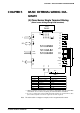
CHAPTER 5: BASIC EXTERNAL WIRING DIAGRAM
BASIC EXTERNAL WIRING DIA-
GRAM
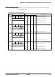
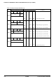
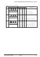
(1) Piezo Buzzer Single Terminal Driving
(Piezo buzzer driving through PNP transistor)
CHAPTER 5
CA
CB
CC
CD
V
V
V
V
V
OSC1
OSC2
OSC3
OSC4
V
RESET
TEST
Vss
C1
C2
C3
C4
C5
C6
C7
C
X'tal
L1
L2
L3
L4
DD
S1
1.5V
or
3.0V
Piezo
Buzzer
R12
MO
K00
K03
K10
P00
P03
CMPP
CMPM
R00
R03
R10
R11
I
I/O
O
SEG0
COM7/SEG38
COM6/SEG39
COM5/SEG40
COM4/SEG41
COM3
COM0
LCD
PANEL
S1C62N82
S1C62L82
S1C62A82
O
Coil
GX
Cp
Ceramic
C
GC
C
DC
C8
*1
*2
*2
R
CR1
R
CR3
X'tal
R
Ceramic
R
C , C
C
C1–C8
Cp
Crystal oscillator
CR oscillation resistor
Ceramic oscillator
CR oscillation resistor
Capacitor
Trimmer capacitor
Capacitor
Capacitor
32,768 Hz CI(MAX)=35 k
850 k
1 MHz (Typ.)
35 k
100 pF
5–25 pF
0.1 F
3.3 F
Ω
CR1
CR3
GC
GX
µ
µ
DC
Ω
Ω
*1 OSC3 oscillation circuit can be used only for S1C62A82. For the S1C62N82
and 62L82, do not connect anything to terminals OSC3 and OSC4.
*2 In case 1/4 duty was selected with the mask option, set CD and VL4 to N.C.
(not connected). The C3 and C7 capacitor are not required.
The above table is simply an example, and is not guaranteed to work.
Note