S1D13504 Color Graphics LCD/CRT Controller S1D13504 TECHNICAL MANUAL Document Number: X19A-Q-002-14 Copyright © 1997, 2001 Epson Research and Development, Inc. All Rights Reserved. Information in this document is subject to change without notice.You may download and use this document, but only for your own use in evaluating Seiko Epson/EPSON products. You may not modify the document. Epson Research and Development, Inc.
Page 2 Epson Research and Development Vancouver Design Center THIS PAGE LEFT BLANK S1D13504 X19A-Q-002-14 TECHNICAL MANUAL Issue Date: 01/04/18
Epson Research and Development Vancouver Design Center Page 3 Customer Support Information Comprehensive Support Tools Seiko Epson Corp. provides to the system designer and computer OEM manufacturer a complete set of resources and tools for the development of graphics systems. Evaluation / Demonstration Board • Assembled and fully tested graphics evaluation board with installation guide and schematics. • To borrow an evaluation board, please contact your local Seiko Epson Corp. sales representative.
Page 4 Epson Research and Development Vancouver Design Center THIS PAGE LEFT BLANK S1D13504 X19A-Q-002-14 TECHNICAL MANUAL Issue Date: 01/04/18
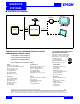
ENERGY S AV I NG EPSON GRAPHICS S1D13504 S1D13504 COLOR GRAPHICS LCD/CRT CONTROLLER February 2001 ■ DESCRIPTION The S1D13504 is a low cost, low power, color/monochrome LCD/CRT controller interfacing to a wide range of CPUs and LCDs. The S1D13504 architecture is designed to meet the requirements of embedded markets such as Office Automation equipment, Mobile Communications devices and Hand-Held PCs where Windows CE may serve as a primary operating system.
GRAPHICS S1D13504 ■ SYSTEM BLOCK DIAGRAM RAMDAC EDO-DRAM FPM-DRAM Analog Out CRT Control CPU Clock S1D13504 Digital Out Flat Panel CONTACT YOUR SALES REPRESENTATIVE FOR THESE COMPREHENSIVE DESIGN TOOLS: • S1D13504 Technical Manual • S5U13504 Evaluation Boards • Windows CE Display Driver • CPU Independent Software Utilities Japan Seiko Epson Corporation Electronic Devices Marketing Division 421-8, Hino, Hino-shi Tokyo 191-8501, Japan Tel: 042-587-5812 Fax: 042-587-5564 http://www.epson.co.
S1D13504 Color Graphics LCD/CRT Controller Hardware Functional Specification Document Number: X19A-A-002-18 Copyright © 1997, 2001 Epson Research and Development, Inc. All Rights Reserved. Information in this document is subject to change without notice.You may download and use this document, but only for your own use in evaluating Seiko Epson/EPSON products. You may not modify the document. Epson Research and Development, Inc.
Page 2 Epson Research and Development Vancouver Design Center THIS PAGE LEFT BLANK S1D13504 X19A-A-002-18 Hardware Functional Specification Issue Date: 01/01/30
Epson Research and Development Vancouver Design Center Page 3 Table of Contents 1 2 Introduction . . . . . . . . . . . . . . . . . . . . . . . . . . . . . . . . . . . . . . . . . . . . 11 1.1 Scope . . . . . . . . . . . . . . . . . . . . . . . . . . . . . . . . . . . . . 11 1.2 Overview Description . . . . . . . . . . . . . . . . . . . . . . . . . . . . . . . 11 Features . . . . . . . . . . . . . . . . . . . . . . . . . . . . . . . . . . . . . . . . . . . . . . 12 2.1 Memory Interface . . . . . .
Page 4 Epson Research and Development Vancouver Design Center 7.1.2 MC68K Bus 1 Interface Timing (e.g. MC68000) . . . . . . . . . . . . . . . . . . . . . . . .38 7.1.3 MC68K Bus 2 Interface Timing (e.g. MC68030) . . . . . . . . . . . . . . . . . . . . . . . .40 7.1.4 Generic MPU Interface Synchronous Timing . . . . . . . . . . . . . . . . . . . . . . . . . .42 7.1.5 Generic MPU Interface Asynchronous Timing . . . . . . . . . . . . . . . . . . . . . . . . .44 7.2 Clock Input Requirements . . . . .
Epson Research and Development Vancouver Design Center 8.2.9 9 Page 5 External RAMDAC Control Registers . . . . . . . . . . . . . . . . . . . . . . . . . . . . 112 Display Buffer . . . . . . . . . . . . . . . . . . . . . . . . . . . . . . . . . . . . . . . . . . . 114 9.1 Image Buffer . . . . . . . . . . . . . . . . . . . . . . . . . . . . . . . . . . .115 9.2 Half Frame Buffer . . . . . . . . . . . . . . . . . . . . . . . . . . . . . . . . 115 10 Display Configuration . . . . . . . . . . . . . . .
Page 6 Epson Research and Development Vancouver Design Center THIS PAGE LEFT BLANK S1D13504 X19A-A-002-18 Hardware Functional Specification Issue Date: 01/01/30
Epson Research and Development Vancouver Design Center Page 7 List of Tables Table 2-1: S1D13504 Series Package list . . . . . . . . . . . . . . . . . . . . . . . . . . . . . . . . . . . . 13 Table 5-1: Host Interface Pin Descriptions . . . . . . . . . . . . . . . . . . . . . . . . . . . . . . . . . . . 22 Table 5-2: Memory Interface Pin Descriptions . . . . . . . . . . . . . . . . . . . . . . . . . . . . . . . . . 25 Table 5-3: LCD Interface Pin Descriptions . . . . . . . . . . . . . . . . . . . .
Page 8 Epson Research and Development Vancouver Design Center Table 7-25: Dual Monochrome 8-Bit Panel A.C. Timing . . . . . . . . . . . . . . . . . . . . . . . . . . . . .78 Table 7-26: Dual Color 8-Bit Panel A.C. Timing . . . . . . . . . . . . . . . . . . . . . . . . . . . . . . . . .80 Table 7-27: Dual Color 16-Bit Panel A.C. Timing . . . . . . . . . . . . . . . . . . . . . . . . . . . . . . . .82 Table 7-28: TFT A.C. Timing . . . . . . . . . . . . . . . . . . . . . . . . . . . . . . . . . . . . . . . .
Epson Research and Development Vancouver Design Center Page 9 List of Figures Figure 3-1: Typical System Diagram – SH-3 Bus, 1Mx16 FPM/EDO-DRAM . . . . . . . . . . . . . . . . . 14 Figure 3-2: Typical System Diagram – MC68K Bus 1, 1Mx16 FPM/EDO-DRAM (16-Bit MC68000) . . . . 15 Figure 3-3: Typical System Diagram – MC68K Bus 2, 256Kx16 FPM/EDO-DRAM (32-Bit MC68030) . . 15 Figure 3-4: Typical System Diagram – Generic Bus, 1Mx16 FPM/EDO-DRAM . . . . . . . . . . . . . . .
Page 10 Epson Research and Development Vancouver Design Center Figure 7-33: Dual Color 8-Bit Panel Timing . . . . . . . . . . . . . . . . . . . . . . . . . . . . . . . . . . . 79 Figure 7-34: Dual Color 8-Bit Panel A.C. Timing . . . . . . . . . . . . . . . . . . . . . . . . . . . . . . . . 80 Figure 7-35: Dual Color 16-Bit Panel Timing . . . . . . . . . . . . . . . . . . . . . . . . . . . . . . . . . . . 81 Figure 7-36: Dual Color 16-Bit Panel A.C. Timing . . . . . . . . . . . . . . . . . . . . . . . . .
Epson Research and Development Vancouver Design Center Page 11 1 Introduction 1.1 Scope This is the Functional Specification for the S1D13504 Series Color Graphics LCD/CRT Controller Chip. Included in this document are timing diagrams, AC and DC characteristics, register descriptions, and power management descriptions. This document is intended for two audiences: Video Subsystem Designers and Software Developers. 1.
Page 12 Epson Research and Development Vancouver Design Center 2 Features 2.1 Memory Interface • 16-bit DRAM interface: • EDO-DRAM up to 40MHz data rate (80M bytes per second). • FPM-DRAM up to 25MHz data rate (50M bytes per second). • Memory size options: • 512K bytes using one 256K×16 device. • 2M bytes using one 1M×16 device. • A configuration register can be programmed to enhance performance by tailoring the memory control output timing to the DRAM device. 2.
Epson Research and Development Vancouver Design Center Page 13 2.4 Display Modes • 1/2/4/8/16 bit-per-pixel modes supported on LCD. • 1/2/4/8 bit-per-pixel modes supported on CRT. • Up to 16 shades of gray by FRM on monochrome passive LCD panels; a 16x4 Look-Up Table is used to map 1/2/4 bit-per-pixel modes into these shades.
Page 14 Epson Research and Development Vancouver Design Center Power Management Oscillator SUSPEND# CLKI 3 Typical System Implementation Diagrams SH-3 BUS A21 CSn# M/R# CS# A[20:0] AB[20:0] D[15:0] DB[15:0] WE1# BS# RD/WR# RD# WE1# BS# S1D13504 RD/WR# WE0# WAIT# WAIT# UD[7:0] FPDAT[7:0] LD[7:0] FPSHIFT FPSHIFT 4/8/16-bit FPFRAME FPFRAME LCD Display FPLINE RD# WE0# FPDAT[15:8] FPLINE DRDY MOD RAS# LCAS# UCAS# LCAS# UCAS# WE# RAS# MD[15:0] WE# RESET# MA[11:0] R
Epson Research and Development Vancouver Design Center Page 15 .
Page 16 Epson Research and Development Vancouver Design Center Power Management Oscillator SUSPEND# CLKI .
Epson Research and Development Vancouver Design Center Page 17 4 Block Description 4.1 Functional Block Diagram 16-bit FPM/EDO DRAM Memory Controller Register Power Save Clocks CPU R/W LCD Display FIFO Host CPU / MPU I/F I/F LCD DAC Data Look-Up Table DAC Control CRTC Bus Clock Memory Clock Pixel Clock Figure 4-1: System Block Diagram Showing Datapaths 4.2 Functional Block Descriptions 4.2.
Page 18 Epson Research and Development Vancouver Design Center 4.2.4 Look-Up Table The Look-Up Table block contains three 16x4 Look-Up Tables, one for each primary color. In monochrome mode only one of these Look-Up Tables is selected and used. 4.2.5 LCD Interface The LCD Interface block performs frame rate modulation for passive LCD panels. It also generates the correct data format and timing control signals for various LCD and TFT panels. 4.2.
Epson Research and Development Vancouver Design Center Page 19 5 Pin Out 5.
Page 20 Epson Research and Development Vancouver Design Center 5.
Epson Research and Development Vancouver Design Center Page 21 5.
Page 22 Epson Research and Development Vancouver Design Center 5.4 Pin Description Key: I = Input O = Output IO = Bi-Directional (Input/Output) P = Power pin C = CMOS level input CD = CMOS level input with pull-down resistor (typical values of 100KΩ/180KΩ at 5V/3.3V respectively) CS = CMOS level Schmitt input COx = CMOS output driver, x denotes driver type (1=3/-1.5mA, 2=6/-3mA, 3=12/-6mA) TSx = Tri-state CMOS output driver, x denotes driver type (1=3/-1.
Epson Research and Development Vancouver Design Center Page 23 Table 5-1: Host Interface Pin Descriptions (Continued) Pin Name Pin # F00A F02A F01A Type Driver Reset = 0 Value Description This pin has multiple functions. WE1# I 9 11 CS Hi-Z • For SH-3 mode, this pin inputs the write enable signal for the upper data byte (WE1#). • For MC68K Bus 1, this pin inputs the upper data strobe (UDS#). • For MC68K Bus 2, this pin inputs the data strobe (DS#).
Page 24 Epson Research and Development Vancouver Design Center Table 5-1: Host Interface Pin Descriptions (Continued) Pin Name Pin # F00A F02A F01A Type Driver Reset = 0 Value Description This pin has multiple functions. WE0# I 8 10 CS Hi-Z • For SH-3 mode, this pin inputs the write enable signal for the lower data byte (WE0#). • For MC68K Bus 1, this pin must be tied to IO VDD. • For MC68K Bus 2, this pin inputs the bus size bit 0 (SIZ0).
Epson Research and Development Vancouver Design Center Page 25 5.4.2 Memory Interface Table 5-2: Memory Interface Pin Descriptions Pin # Pin Name Type F00A F01A F02A Driver Reset = 0 Value Description This pin has multiple functions. LCAS# O 50 56 CO1 Output 1 • For dual CAS# DRAM, this is the column address strobe for the lower byte (LCAS#). • For single CAS# DRAM, this is the column address strobe (CAS#). See Table 5-10: “Memory Interface Pin Mapping,” on page 32 for summary.
Page 26 Epson Research and Development Vancouver Design Center Table 5-2: Memory Interface Pin Descriptions (Continued) Pin # Pin Name Type MA[8:0] O F00A F01A F02A 43, 41, 39, 37, 35, 34, 36, 38, 40 46, 44, 42, 40, 41, 43, 45, 47, 49 Driver CO1 Reset = 0 Value Output 0 Description Multiplexed memory address. This pin has multiple functions. MA9 IO 45 51 C/TS1 • For 2M byte DRAM, this is memory address bit 9 (MA9). • For asymmetrical 512K byte DRAM, this is memory address bit 9 (MA9).
Epson Research and Development Vancouver Design Center Page 27 5.4.3 LCD Interface Table 5-3: LCD Interface Pin Descriptions Pin # Pin Name Type FPDAT[8:0] O Driver F00A F!A F02A 88, 82-75 98, 92-85 CN3 Reset = 0 Value Description Output 0 Panel Data These pins have multiple functions. FPDAT[15:9] O 95-89 105-99 CN3 • Panel Data for 16-bit panels. Output 0 • Pixel Data for external RAMDAC support. See Table 5-11: “LCD, CRT, RAMDAC Interface Pin Mapping,” on page 33.
Page 28 Epson Research and Development Vancouver Design Center 5.4.5 CRT and External RAMDAC Interface Table 5-5: CRT and RAMDAC Interface Pin Descriptions Pin # Pin Name Type F00A F01A F02A Driver Reset = 0 Value Description This pin has multiple functions. DACRD# IO 84 94 C/TS1 • Read signal for external RAMDAC support. Hi-Z / • General Purpose IO (GPIO4). Output 11 See Table 5-11: “LCD, CRT, RAMDAC Interface Pin Mapping,” on page 33. This pin has multiple functions.
Epson Research and Development Vancouver Design Center Page 29 Table 5-5: CRT and RAMDAC Interface Pin Descriptions (Continued) Pin # Pin Name Type F00A F01A F02A Driver Reset = 0 Value Description This pin has multiple functions. HRTC IO 102 116 C/CN3 • Horizontal Retrace signal for CRT. Hi-Z / 1 • General Purpose IO (GPIO10). Output 0 See Table 5-11: “LCD, CRT, RAMDAC Interface Pin Mapping,” on page 33. This pin has multiple functions.
Page 30 Epson Research and Development Vancouver Design Center 5.4.6 Miscellaneous Table 5-6: Miscellaneous Pin Descriptions Pin # Pin Name Type F00A F01A Driver F02A Reset = 0 Value Description This pin has multiple functions. • When MD9 = 0 at rising edge of RESET#, this pin is an active-low input used to place the S1D13504 into suspend mode; see Section 13, “Power Save Modes” on page 128 for details. • When MD[10:9] = 01 at rising edge of RESET#, this pin is an output with a reset state of 0.
Epson Research and Development Vancouver Design Center Page 31 5.5 Summary of Configuration Options Table 5-8: Summary of Power On / Reset Options value on this pin at rising edge of RESET# is used to configure: Pin Name 1 (1/0) 0 MD0 8-bit host bus interface MD[3:1] Select host bus interface: 000 = SH-3 bus interface 001 = MC68K bus 1 (e.g. MC68000) 010 = MC68K bus 2 (e.g. MC68030) 011 = Generic bus interface (e.g.
Page 32 Epson Research and Development Vancouver Design Center 5.
Epson Research and Development Vancouver Design Center Page 33 Table 5-11: LCD, CRT, RAMDAC Interface Pin Mapping Monochrome Passive Panel S1D13504 Pin Names Single 4-bit 8-bit Color Passive Panel Dual Single 8-bit 4-bit Single Single Format 1 Format 2 8-bit 8-bit Color TFT Panel CRT Dual 8-bit 16-bit 9-bit 12-bit 18-bit1 FPFRAME FPFRAME Note2 FPLINE FPLINE Note2 FPSHIFT FPSHIFT Note2 DRDY MOD FPSHIFT2 MOD Note2 DRDY FPDAT0 driven 0 D0 LD0 driven 0 D0 D0 LD0 LD0
Page 34 Epson Research and Development Vancouver Design Center 6 D.C. Characteristics Table 6-1: Absolute Maximum Ratings Symbol Parameter Rating Units Core VDD Supply Voltage VSS - 0.3 to 4.6 V IO VDD Supply Voltage VSS - 0.3 to 6.0 V VIN Input Voltage VSS - 0.3 to IO VDD + 0.5 V VOUT Output Voltage VSS - 0.3 to IO VDD + 0.5 V TSTG Storage Temperature -65 to 150 °C TSOL Solder Temperature/Time 260 for 10 sec.
Epson Research and Development Vancouver Design Center Page 35 Table 6-4: Output Specifications Symbol Parameter Condition VOL Low Level Output Voltage Type 1 - TS1, CO1, TS1D Type 2 - TS2, CO2 Type 3 - TS3, CO3 IOL = 3mA IOL = 6mA IOL = 12mA VOH High Level Output Voltage Type 1 - TS1, CO1, TS1D Type 2 - TS2, CO2 Type 3 - TS3, CO3 IOL = -1.5 mA IOL = -3 mA IOL = -6 mA IOZ Output Leakage Current COUT CBID IO VDD = Max VOH = VDD VOL = VSS Min Typ Max 0.4 IO VDD - 0.
Page 36 Epson Research and Development Vancouver Design Center 7 A.C. Characteristics Conditions: IO VDD = 2.7V to 5.5V unless otherwise specified TA = -40° C to 85° C Trise and Tfall for all inputs must be ≤ 5 nsec (10% ~ 90%) CL = 50pF (Bus / MPU Interface) CL = 100pF (LCD Panel Interface) CL = 10pF (Display Buffer Interface) CL = 10pF (CRT / DAC Interface) 7.1 CPU Interface Timing 7.1.
Epson Research and Development Vancouver Design Center Page 37 Table 7-1: SH-3 Interface Timing Symbol Parameter Min Max Units t1 Clock period 25 ns t2 Clock pulse width high 5 ns t3 Clock pulse width low 5 ns t4 A[20:0], M/R#, RD/WR# setup to CKIO 4 ns t5 A[20:0], M/R#, RD/WR# hold from CS# 0 ns t6 BS# setup 3 ns t7 BS# hold 0 ns t8 CSn# setup 0 ns t9 Falling edge RD# to D[15:0] driven 3 ns t10 2 Rising edge CSn# to WAIT# tri-state 0 4 ns t111 Falling edge
Page 38 Epson Research and Development Vancouver Design Center 7.1.2 MC68K Bus 1 Interface Timing (e.g.
Epson Research and Development Vancouver Design Center Page 39 Table 7-2: MC68K Bus 1 Interface Timing Symbol Parameter t1 Clock period t2 Min Max 30 Units ns Clock pulse width high 5 ns t3 Clock pulse width low 5 ns t4 A[20:1], M/R# setup to first CLK where CS# = 0 AS# = 0, and either UDS#=0 or LDS# = 0 4 ns t5 A[20:1], M/R# hold from AS# 0 ns t6 CS# hold from AS# 0 ns t7 R/W# setup to before to either UDS#=0 or LDS# = 0 5 ns t8 R/W# hold from AS# 0 ns 1 AS# = 0 and C
Page 40 Epson Research and Development Vancouver Design Center 7.1.3 MC68K Bus 2 Interface Timing (e.g.
Epson Research and Development Vancouver Design Center Page 41 Table 7-3: MC68K Bus 2 Interface Timing Symbol Parameter t1 Clock period t2 Min Max 30 Units ns Clock pulse width high 5 ns t3 Clock pulse width low 5 ns t4 A[20:0], SIZ[1:0], M/R# setup to first CLK where CS# = 0 AS# = 0, and either UDS#=0 or LDS# = 0 4 ns t5 A[20:0], SIZ[1:0], M/R# hold from AS# 0 ns t6 CS# hold from AS# 0 ns t7 R/W# setup to DS# 5 ns t8 R/W# hold from AS# 0 ns 1 AS# = 0 and CS# = 0 to DS
Page 42 Epson Research and Development Vancouver Design Center 7.1.
Epson Research and Development Vancouver Design Center Page 43 Table 7-4: Generic MPU Interface Synchronous Timing Symbol Parameter Min Max Units Bus clock period 25 ns t1 A[20:0], M/R#, CS#, RD0#,RD1#,WE0#,WE1# hold time 1 ns t2 A[20:0], M/R#, CS#, RD0#,RD1#,WE0#,WE1# setup time 5 ns t3 RD0#,RD1#,WE0#,WE1# high to A[20:0], M/R# invalid and CS# high 0 ns TBCLK 1 RD0#,RD1#,WE0#,WE1# low and CS# low to WAIT# driven low 1 7 ns t5 BCLK to WAIT# high 0 15 ns t6 RD0#,RD1#,WE0#,WE
Page 44 Epson Research and Development Vancouver Design Center 7.1.
Epson Research and Development Vancouver Design Center Page 45 Table 7-5: Generic MPU Interface Asynchronous Timing Symbol Parameter Min Max Units Bus clock period 25 ns t1 RD0#, RD1#, WE0#, WE1# low to CS# low 4 ns t2 A[20:0], M/R# valid to RD0#, RD1#, WE0#, WE1# low 0 ns t3 RD0#, RD1#, WE0#, WE1# high to A[20:0], CS#, M/R# invalid and CS# high 0 ns TBCLK 1 CS# low to WAIT# driven low 1 7 ns t5 RD0#, RD1#, WE0#, WE1# high to WAIT# high impedance 1 6 ns t6 WE0#, WE1# low to
Page 46 Epson Research and Development Vancouver Design Center 7.2 Clock Input Requirements Clock Input Waveform t t PWH PWL V IH VIL TCLKI Figure 7-6: Clock Input Requirements Table 7-6: Clock Input Requirements Symbol TCLKI TPCLK TMCLK tPWH tPWL Parameter Input Clock Period (CLKI) Pixel Clock Period (PCLK) not shown Memory Clock Period (MCLK) not shown Input Clock Pulse Width High (CLKI) Input Clock Pulse Width Low (CLKI) Min 12.
Epson Research and Development Vancouver Design Center Page 47 7.3 Memory Interface Timing 7.3.
Page 48 Epson Research and Development Vancouver Design Center Table 7-7: EDO DRAM Read Timing Symbol t1 t2 t3 Parameter Min Typ Max Units Memory clock period 25 ns Random read or write cycle time (REG[22h] bits [6:5] = 00) 5 t1 ns Random read or write cycle time (REG[22h] bits [6:5] = 01) 4 t1 ns Random read or write cycle time (REG[22h] bits [6:5] = 10) 3 t1 ns Row address setup time (REG[22h] bits [3:2] = 00) 2.
Epson Research and Development Vancouver Design Center Page 49 7.3.
Page 50 Epson Research and Development Vancouver Design Center Table 7-8: EDO DRAM Write Timing Symbol t1 t2 t3 t4 Parameter Min Typ Max Units Memory clock period 25 ns Random read or write cycle time (REG[22h] bits [6:5] = 00) 5 t1 ns Random read or write cycle time (REG[22h] bits [6:5] = 01) 4 t1 ns Random read or write cycle time (REG[22h] bits [6:5] = 10) 3 t1 ns Row address setup time (REG[22h] bits [3:2] = 00) 2.
Epson Research and Development Vancouver Design Center Page 51 7.3.
Page 52 Epson Research and Development Vancouver Design Center Table 7-9: EDO DRAM Read-Write Timing Symbol t1 t2 t3 t4 Parameter Min Typ Max Units Memory clock period 25 ns Random read or write cycle time (REG[22h] bits [6:5] = 00) 5 t1 ns Random read or write cycle time (REG[22h] bits [6:5] = 01) 4 t1 ns Random read or write cycle time (REG[22h] bits [6:5] = 10) 3 t1 ns Row address setup time (REG[22h] bits [3:2] = 00) 2.
Epson Research and Development Vancouver Design Center Page 53 7.3.4 EDO-DRAM CAS Before RAS Refresh Timing t1 Memory Clock t2 t3 RAS# CAS# t4 t5 t6 Figure 7-10: EDO-DRAM CAS Before RAS Refresh Timing Table 7-10: EDO-DRAM CAS Before RAS Refresh Timing Symbol t1 t2 t3 t4 t5 t6 Parameter Min Typ Max Units 25 ns RAS# to CAS# precharge time (REG[22h] bits [3:2] = 00) 1.45 t1 ns RAS# to CAS# precharge time (REG[22h] bits [3:2] = 01 or 10) 0.
Page 54 Epson Research and Development Vancouver Design Center 7.3.5 EDO-DRAM Self-Refresh Timing Stopped for suspend mode t1 Memory Clock Restarted for active mode t5 t2 RAS# CAS# t3 t4 Figure 7-11: EDO-DRAM Self-Refresh Timing Table 7-11: EDO-DRAM Self-Refresh Timing Symbol t1 t2 t3 t4 t5 Parameter Min Typ Max Units 25 ns RAS# to CAS# precharge time (REG[22h] bits [3:2] = 00) 1.45 t1 ns RAS# to CAS# precharge time (REG[22h] bits [3:2] = 01 or 10) 0.
Epson Research and Development Vancouver Design Center Page 55 7.3.
Page 56 Epson Research and Development Vancouver Design Center Table 7-12: FPM DRAM Read Timing Symbol t1 t2 Parameter Min Typ Max Units Memory clock 40 ns Random read or write cycle time (REG[22h] bits [6:5] = 00) 5 t1 ns Random read or write cycle time (REG[22h] bits [6:5] = 01) 4 t1 ns Random read or write cycle time (REG[22h] bits [6:5] = 10) 3 t1 ns Row address setup time (REG[22h] bits [3:2] = 00) 2 t1 ns Row address setup time (REG[22h] bits [3:2] = 01) 1.
Epson Research and Development Vancouver Design Center Page 57 7.3.
Page 58 Epson Research and Development Vancouver Design Center Table 7-13: FPM-DRAM Write Timing Symbol t1 t2 Parameter Min Typ Max Units Memory clock 40 ns Random read or write cycle time (REG[22h] bits [6:5] = 00) 5 t1 ns Random read or write cycle time (REG[22h] bits [6:5] = 01) 4 t1 ns Random read or write cycle time (REG[22h] bits [6:5] = 10) 3 t1 ns Row address setup time (REG[22h] bits [3:2] = 00) 2 t1 ns Row address setup time (REG[22h] bits [3:2] = 01) 1.
Epson Research and Development Vancouver Design Center Page 59 7.3.
Page 60 Epson Research and Development Vancouver Design Center Table 7-14: FPM-DRAM Read-Write Timing Symbol t1 t2 Parameter Min Typ Max Units Memory clock 40 ns Random read or write cycle time (REG[22h] bits [6:5] = 00) 5 t1 ns Random read or write cycle time (REG[22h] bits [6:5] = 01) 4 t1 ns Random read or write cycle time (REG[22h] bits [6:5] = 10) 3 t1 ns Row address setup time (REG[22h] bits [3:2] = 00) 2 t1 ns Row address setup time (REG[22h] bits [3:2] = 01) 1.
Epson Research and Development Vancouver Design Center Page 61 7.3.
Page 62 Epson Research and Development Vancouver Design Center 7.3.
Epson Research and Development Vancouver Design Center Page 63 7.4 Display Interface 7.4.
Page 64 Epson Research and Development Vancouver Design Center 7.4.
Epson Research and Development Vancouver Design Center Page 65 7.4.
Page 66 Epson Research and Development Vancouver Design Center t1 Sync Timing t2 FPFRAME t4 t3 FPLINE t5 MOD Data Timing FPLINE t6 t7 t9 t8 t10 t11 t12 FPSHIFT t13 t14 1 UD[3:0] 2 Figure 7-20: Single Monochrome 4-Bit Panel A.C. Timing Table 7-19: Single Monochrome 4-Bit Panel A.C.
Epson Research and Development Vancouver Design Center Page 67 7.4.
Page 68 Epson Research and Development Vancouver Design Center t1 t2 Sync Timing FPFRAME t4 t3 FPLINE t5 MOD Data Timing FPLINE t6 t7 t9 t8 t10 t11 t12 FPSHIFT t13 UD[3:0] LD[3:0] t14 1 2 Figure 7-22: Single Monochrome 8-Bit Panel A.C. Timing Table 7-20: Single Monochrome 8-Bit Panel A.C. Timing Symbol t1 t2 t3 t4 t5 t6 t7 t8 t9 t10 t11 t12 t13 t14 1. 2. 3. 4. 5. 6.
Epson Research and Development Vancouver Design Center Page 69 7.4.
Page 70 Epson Research and Development Vancouver Design Center t1 t2 Sync Timing FPFRAME t4 t3 FPLINE t5 MOD Data Timing FPLINE t6 t7 t9 t8 t10 t11 t12 FPSHIFT t13 t14 1 UD[3:0] 2 Figure 7-24: Single Color 4-Bit Panel A.C. Timing Table 7-21: Single Color 4-Bit Panel A.C. Timing Symbol Parameter t1 FPFRAME setup to FPLINE falling edge t2 FPFRAME hold from FPLINE falling edge t3 1. 2. 3. 4. 5. 6.
Epson Research and Development Vancouver Design Center Page 71 7.4.
Page 72 Epson Research and Development Vancouver Design Center t1 t2 Sync Timing FPFRAME t4 t3 FPLINE Data Timing FPLINE t5a t5b t6 t8a t7 t9 t10 t11 FPSHIFT t8b FPSHIFT2 t12 UD[3:0] LD[3:0] t13 1 2 Figure 7-26: Single Color 8-Bit Panel A.C. Timing (Format 1) Table 7-22: Single Color 8-Bit Panel A.C. Timing (Format 1) Symbol t1 1. 2. 3. 4. 5. 6. 7.
Epson Research and Development Vancouver Design Center Page 73 7.4.
Page 74 Epson Research and Development Vancouver Design Center t1 Sync Timing t2 FPFRAME t3 t4 FPLINE t5 MOD Data Timing FPLINE t6 t8 t7 t9 t14 t11 t10 FPSHIFT t12 UD[3:0] LD[3:0] t13 1 2 Figure 7-28: Single Color 8-Bit Panel A.C. Timing (Format 2) Table 7-23: Single Color 8-Bit Panel A.C.
Epson Research and Development Vancouver Design Center Page 75 7.4.
Page 76 Epson Research and Development Vancouver Design Center t1 Sync Timing t2 FPFRAME t3 t4 FPLINE t5 MOD Data Timing FPLINE t6 t8 t7 t9 t14 t10 t11 FPSHIFT t12 UD[7:0] LD[7:0] t13 1 2 Figure 7-30: Single Color 16-Bit Panel A.C. Timing Table 7-24: Single Color 16-Bit Panel A.C. Timing Symbol t1 1. 2. 3. 4. 5. 6.
Epson Research and Development Vancouver Design Center Page 77 7.4.
Page 78 Epson Research and Development Vancouver Design Center t1 Sync Timing t2 FPFRAME t4 t3 FPLINE t5 MOD Data Timing FPLINE t6 t8 t7 t9 t14 t10 t11 FPSHIFT t12 t13 1 UD[3:0] LD[3:0] 2 Figure 7-32: Dual Monochrome 8-Bit Panel A.C. Timing Table 7-25: Dual Monochrome 8-Bit Panel A.C. Timing Symbol t1 t2 t3 t4 t5 t6 t7 t8 t9 t10 t11 t12 t13 t14 1. 2. 3. 4. 5. 6.
Epson Research and Development Vancouver Design Center Page 79 7.4.
Page 80 Epson Research and Development Vancouver Design Center t1 t2 Sync Timing FPFRAME t4 t3 FPLINE t5 MOD Data Timing FPLINE t6 t8 t7 t9 t14 t11 t10 FPSHIFT t12 UD[3:0] LD[3:0] t13 1 2 Figure 7-34: Dual Color 8-Bit Panel A.C. Timing Table 7-26: Dual Color 8-Bit Panel A.C.
Epson Research and Development Vancouver Design Center Page 81 7.4.
Page 82 Epson Research and Development Vancouver Design Center t1 t2 Sync Timing FPFRAME t4 t3 FPLINE t5 MOD Data Timing FPLINE t6 t8 t7 t9 t14 t11 t10 FPSHIFT t12 UD[7:0] LD[7:0] t13 1 2 Figure 7-36: Dual Color 16-Bit Panel A.C. Timing Table 7-27: Dual Color 16-Bit Panel A.C. Timing Symbol t1 FPFRAME setup to FPLINE falling edge t2 FPFRAME hold from FPLINE falling edge 1. 2. 3. 4. 5. 6.
Epson Research and Development Vancouver Design Center Page 83 7.4.
Page 84 Epson Research and Development Vancouver Design Center t8 t9 FPFRAME t12 FPLINE t6 FPLINE t15 t7 t17 DRDY t14 t1 t2 t3 t11 t13 t16 FPSHIFT t4 R[5:1] G[5:0] B[5:1] t5 1 2 639 640 t10 Note: DRDY is used to indicate the first pixel Figure 7-38: TFT A.C.
Epson Research and Development Vancouver Design Center Page 85 Table 7-28: TFT A.C. Timing Symbol t1 FPSHIFT period Min 1 t2 FPSHIFT pulse width high 0.45 Ts t3 FPSHIFT pulse width low 0.45 Ts t4 data setup to FPSHIFT falling edge 0.45 Ts t5 data hold from FPSHIFT falling edge 0.
Page 86 Epson Research and Development Vancouver Design Center 7.4.
Epson Research and Development Vancouver Design Center Page 87 t8 t9 VRTC t12 HRTC t6 HRTC t15 t7 BLANK# t14 t1 t2 t3 t11 t13 t16 DACCLK t4 DACD[7:0] t5 1 2 639 640 t10 Figure 7-40: CRT A.C.
Page 88 Epson Research and Development Vancouver Design Center Table 7-29: CRT A.C. Timing Symbol 1. 2. 3. 4. 5. 6. 7. 8. 9. Parameter t1 DACCLK period Min 1 t2 DACCLK pulse width high 0.45 Ts t3 DACCLK pulse width low 0.45 Ts t4 data setup to DACCLK rising edge 0.45 Ts t5 data hold from DACCLK rising edge 0.
Epson Research and Development Vancouver Design Center Page 89 7.4.
Page 90 Epson Research and Development Vancouver Design Center 8 Registers 8.1 Register Mapping The S1D13504 registers are all memory mapped. The system must provide the external address decoding through the CS# and M/R# input pins. When CS# = 0 and M/R# = 0, the registers are mapped by address bits AB[5:0], e.g. REG[00h] is mapped to AB[5:0] = 000000, REG[01h] is mapped to AB[5:0] = 000001.
Epson Research and Development Vancouver Design Center Page 91 8.2.2 Memory Configuration Registers Memory Configuration Register REG[01h] n/a RW Refresh Rate Bit 2 bits 6-4 Refresh Rate Bit 1 Refresh Rate Bit 0 n/a WE# Control n/a Memory Type DRAM Refresh Rate Select Bits [2:0] These bits specify the amount of divide from the input clock (CLKI) to generate the DRAM refresh clock rate, which is equal to 2(ValueOfTheseBits + 6).
Page 92 Epson Research and Development Vancouver Design Center 8.2.3 Panel/Monitor Configuration Registers Panel Type Register REG[02h] n/a RW Panel Data Width Bit 1 n/a bits 5-4 Panel Data Width Bit 0 Panel Data Color/Mono Format Select Panel Select Dual/Single Panel Select TFT/Passive LCD Panel Select Panel Data Width Bits [1:0] These bits select passive LCD/TFT panel data width size.
Epson Research and Development Vancouver Design Center Page 93 Horizontal Display Width Register REG[04h] n/a RW Horizontal Horizontal Horizontal Horizontal Horizontal Horizontal Horizontal Display Width Display Width Display Width Display Width Display Width Display Width Display Width Bit 6 Bit 5 Bit 4 Bit 3 Bit 2 Bit 1 Bit 0 bits 6-0 Horizontal Display Width Bits [6:0] These bits specify the LCD panel and/or the CRT horizontal display width as follows.
Page 94 Epson Research and Development Vancouver Design Center HRTC/FPLINE Pulse Width Register REG[07h] HRTC Polarity Select RW FPLINE Polarity Select n/a HRTC/ HRTC/ HRTC/ HRTC/ FPLINE Pulse FPLINE Pulse FPLINE Pulse FPLINE Pulse Width Bit 3 Width Bit 2 Width Bit 1 Width Bit 0 n/a bit 7 HRTC Polarity Select For CRTs, this bit selects the polarity of the HRTC. When this bit = 1, the HRTC pulse is active high. When this bit = 0, the HRTC pulse is active low.
Epson Research and Development Vancouver Design Center Page 95 Vertical Non-Display Period Register REG[0Ah] Vertical Non-Display Period Status (RO) RW Vertical Non-Display Period Bit 5 n/a bit 7 Vertical Non-Display Period Bit 4 Vertical Non-Display Period Bit 3 Vertical Non-Display Period Bit 2 Vertical Non-Display Period Bit 1 Vertical Non-Display Period Bit 0 Vertical Non-Display Period Status This is a read-only status bit. A “1” indicates that a vertical non-display period is occurring.
Page 96 Epson Research and Development Vancouver Design Center VRTC/FPFRAME Pulse Width Register REG[0Ch] RW FPFRAME VRTC Polarity Polarity Select Select n/a n/a n/a VRTC/ FPFRAME Pulse Width Bit 2 VRTC/ FPFRAME Pulse Width Bit 1 VRTC/ FPFRAME Pulse Width Bit 0 bit 7 VRTC Polarity Select For CRTs, this bit selects the polarity of the VRTC. When this bit = 1, the VRTC pulse is active high. When this bit = 0, the VRTC pulse is active low.
Epson Research and Development Vancouver Design Center Page 97 8.2.
Page 98 bits 4-2 Epson Research and Development Vancouver Design Center Number of Bits-Per-Pixel Select Bits [2:0] These bits select the number of bits-per-pixel (bpp) for the displayed data. Note 15 and 16-bpp modes bypass the LUT and are supported as 12-bpp on passive panels and 15/16bpp on TFT panels. These modes are not supported on CRT. See Figure 10-2: “15/16 Bit-PerPixel Format Memory Organization,” on page 117 for a description of passive panel support.
Epson Research and Development Vancouver Design Center Page 99 Screen 1 Line Compare Register 0 REG[0Eh] RW Screen 1 Line Screen 1 Line Screen 1 Line Screen 1 Line Screen 1 Line Screen 1 Line Screen 1 Line Screen 1 Line Compare Bit 7 Compare Bit 6 Compare Bit 5 Compare Bit 4 Compare Bit 3 Compare Bit 2 Compare Bit 1 Compare Bit 0 Screen 1 Line Compare Register 1 REG[0Fh] n/a RW n/a REG[0Eh] bits 7-0 REG[0Fh] bits 1-0 n/a n/a n/a n/a Screen 1 Line Screen 1 Line Compare Bit 9 Compare Bit 8 Screen
Page 100 Epson Research and Development Vancouver Design Center Screen 2 Display Start Address Register 0 RW REG[13h] RW Start Address Start Address Start Address Start Address Start Address Start Address Start Address Start Address Bit 7 Bit 6 Bit 5 Bit 4 Bit 3 Bit 2 Bit 1 Bit 0 Screen 2 Display Start Address Register 1 REG[14h] RW Start Address Start Address Start Address Start Address Start Address Start Address Start Address Start Address Bit 15 Bit 14 Bit 13 Bit 12 Bit 11 Bit 10 Bit 9 Bit 8 Scr
Epson Research and Development Vancouver Design Center Page 101 b Pixel Panning Register REG[18h] RW Screen 2 Screen 2 Screen 2 Screen 2 Screen 1 Screen 1 Screen 1 Screen 1 Pixel Panning Pixel Panning Pixel Panning Pixel Panning Pixel Panning Pixel Panning Pixel Panning Pixel Panning Bit 3 Bit 2 Bit 1 Bit 0 Bit 3 Bit 2 Bit 1 Bit 0 This register is used to control the horizontal pixel panning of screen 1 and screen 2.
Page 102 Epson Research and Development Vancouver Design Center 8.2.6 Power Save Configuration Registers Power Save Configuration Register REG[1Ah] n/a RW n/a n/a n/a LCD Power Disable Suspend Refresh Select Bit 1 Suspend Refresh Select Bit 0 Software Suspend Mode Enable bit 3 LCD Power Disable When this bit = 1 the LCDPWR output is directly forced to the Off state. The LCDPWR “On/Off” state is configured by MD10 at the rising edge of RESET#.
Epson Research and Development Vancouver Design Center bit 0 Page 103 Half Frame Buffer Disable This bit is used to disable the Half Frame Buffer. When this bit = 1, the Half Frame Buffer is disabled. When this bit = 0, the Half Frame Buffer is enabled. When a single panel is selected, the Half Frame Buffer is automatically disabled and this bit has no hardware effect. The Half Frame Buffer is needed to fully support dual panels.
Page 104 Epson Research and Development Vancouver Design Center bit 5 GPIO5 Pin IO Configuration When this bit = 1, GPIO5 is configured as an output. When this bit = 0 (default), GPIO5 is configured as an input. Note the MD8 pin must be high at the rising edge of RESET# to enable GPIO5, otherwise the BLANK# pin is controlled automatically and this bit will have no effect on hardware. bit 4 GPIO4 Pin IO Configuration When this bit = 1, GPIO4 is configured as an output.
Epson Research and Development Vancouver Design Center Page 105 GPIO Configuration Register 1 REG[1Fh] n/a RW n/a n/a n/a GPIO11 Pin IO Config. GPIO10 Pin IO Config. GPIO9 Pin IO Config. GPIO8 Pin IO Config. bit 3 GPIO11 Pin IO Configuration When this bit = 1, GPIO11 is configured as an output. When this bit = 0 (default), GPIO11 is configured as an input.
Page 106 Epson Research and Development Vancouver Design Center GPIO Status / Control Register 0 REG[20h] GPIO7 Pin IO Status RW GPIO6 Pin IO Status GPIO5 Pin IO Status GPIO4 Pin IO Status GPIO3 Pin IO Status GPIO2 Pin IO Status GPIO1 Pin IO Status GPIO0 Pin IO Status bit 7 GPIO7 Pin IO Status When GPIO7 is configured as an output, a “1” in this bit drives GPIO7 to high and a “0” in this bit drives GPIO7 to low.
Epson Research and Development Vancouver Design Center Page 107 GPIO Status / Control Register 1 REG[21h] GPO Control bit 7 n/a n/a RW n/a GPIO11 Pin IO Status GPIO10 Pin IO Status GPIO9 Pin IO Status GPIO8 Pin IO Status GPO Control This bit is used to control the state of the SUSPEND# pin when it is configured as GPO.
Page 108 Epson Research and Development Vancouver Design Center Performance Enhancement Register 0 REG[22h] EDO ReadWrite Delay RW RC Timing Value Bit 1 RC Timing Value Bit 0 RAS# Precharge Timing Bit 1 RAS# to CAS# Delay RAS# Precharge Timing Bit 0 n/a Reserved Note Changing this register to non-zero value, or to a different non-zero value, should be done only when there are no read/write DRAM cycles.
Epson Research and Development Vancouver Design Center Page 109 Note that for EDO-DRAM and NRP = 1.5, this bit is automatically forced to 0 to select 2 MCLK for NRCD. This is done to satisfy the CAS# address setup time, tASC. The resulting tRC is related to NRCD as follows: tRC tRC tRC tRC = (NRCD) TM = (1.5) TM = (NRCD + 0.5) TM = (NRCD) TM if EDO and NRP = 1 or 2 if EDO and NRP = 1.5 if FPM and NRP = 1 or 2 if FPM and NRP = 1.
Page 110 Epson Research and Development Vancouver Design Center Performance Enhancement Register 1 REG[23h] Display FIFO Disable n/a n/a Display FIFO Threshold Bit 4 Display FIFO Threshold Bit 3 Display FIFO Threshold Bit 2 Display FIFO Threshold Bit 1 Display FIFO Threshold Bit 0 bit 7 Display FIFO Disable When this bit = 1 the display FIFO is disabled and all data outputs are forced to zero (i.e. the screen is blanked). This allows the S1D13504 to be dedicated to service CPU to memory accesses.
Epson Research and Development Vancouver Design Center bits 3-0 Page 111 LUT Address Bits [3:0] These 4 bits provide a pointer into the 16 position Look-Up Table currently selected for CPU read/write access. The Look-Up Table configuration (e.g. 1/2/4 banks) does not affect the read/write access from the CPU as all 16 positions can be accessed sequentially.
Page 112 Epson Research and Development Vancouver Design Center 8.2.9 External RAMDAC Control Registers Note 1. In a Little-Endian architecture, the RAMDAC should be connected to the low byte of the CPU data bus and the following registers are accessed at the lower address given for each register (28h, 2Ah, 2Ch, and 2Eh).
Epson Research and Development Vancouver Design Center Page 113 RAMDAC Palette Data Register REG[2Eh] or REG[2Fh] RAMDAC Data Bit 7 bits 7-0 RW RAMDAC Data Bit 6 RAMDAC Data Bit 5 RAMDAC Data Bit 4 RAMDAC Data Bit 3 RAMDAC Data Bit 2 RAMDAC Data Bit 1 RAMDAC Data Bit 0 RAMDAC Palette Data Bits [7:0] A CPU read or write to this register will generate a DACRD# or DACWR# pulse and DACRS1 = 0 and DACRS0 = 1 to the external RAMDAC for a palette data register access.
Page 114 Epson Research and Development Vancouver Design Center 9 Display Buffer The system addresses the display buffer through the CS#, M/R#, and AB[20:0] input pins. When CS# = 0 and M/R# = 1, the display buffer is addressed by bits AB[20:0] as shown in the following table.
Epson Research and Development Vancouver Design Center Page 115 9.1 Image Buffer The image buffer contains the formatted display data - see Section 10.1, “Display Mode Data Format” on page 116. The displayed image(s) may take up only a portion of the image buffer; the remaining area can be used for multiple images - possibly for animation or general storage. See Section 10, “Display Configuration” on page 116 for details on the relationship between the image buffer and the display. 9.
Page 116 Epson Research and Development Vancouver Design Center 10 Display Configuration 10.
Epson Research and Development Vancouver Design Center Page 117 15-bpp: P0 P1 P2 P3 P4 P5 P6 P7 5-5-5 RGB bit 7 bit 0 G02 G01 G00 B04 B03 B02 B01 B00 Byte 0 R0 Byte 1 4 R03 R0 2 R0 1 R00 G0 4 G0 3 Byte 2 G12 G11 G10 B14 B13 B12 B11 B10 Byte 3 R14 R13 R12 R11 R10 G14 G13 TFT Pn = (Rn4-0, Gn 4-0, Bn4-0) Passive Pn = (Rn4-1, Gn 4-1, Bn4-1) Panel Display Display Buffer Host Address 16-bpp: 5-6-5 RGB bit 7 P0 P1 P2 P3 P4 P5 P6 P7 bit 0 Byte 0 G02 G01 G00 B04 B03 B02 B01 B00 Byte 1
Page 118 Epson Research and Development Vancouver Design Center 10.2 Image Manipulation The figure below shows how screen 1 and screen 2 images stored in the image buffer are positioned on the display. The screen 1 and screen 2 images can be parts of a larger virtual image or images. • (REG[17h], REG[16h]) defines the width of the virtual image(s). • (REG[12h], REG[11h], REG[10h]) defines the starting word of the screen 1, (REG[15h], REG[14h], REG[13h]) defines the starting word of the screen 2.
Epson Research and Development Vancouver Design Center Page 119 11 Clocking 11.1 Maximum MCLK: PCLK Ratios Table 11-1: Maximum PCLK Frequency with EDO-DRAM Display type NRC • Single Panel. • CRT. • Dual Monochrome/Color Panel with Half Frame Buffer Disabled. • Simultaneous CRT + Single Panel. • Simultaneous CRT + Dual Monochrome/Color Panel with Half Frame Buffer Disabled. 5, 4, 3 Maximum PCLK Allowed 1 bpp 2 bpp 4 bpp 8 bpp 16 bpp MCLK • Dual Monochrome Panel with Half Frame Buffer Enabled.
Page 120 Epson Research and Development Vancouver Design Center 11.
Epson Research and Development Vancouver Design Center Page 121 Table 11-3: Example Frame Rates DRAM Type1 (Speed Grade) 60ns EDO-DRAM Display • Single Panel. • CRT. • Dual Mono/Color Panel with Half Frame Buffer Disabled.5 • Simultaneous CRT + Single Panel. • Simultaneous CRT + Dual Mono/Color Panel with Half Frame Buffer Disabled.5 800x6002 640x480 640x240 480x320 MClk = 33MHz NRC = 4 NRP = 1.5 NRCD = 2 320x240 • Dual Color with Half Frame Buffer Enabled.
Page 122 Epson Research and Development Vancouver Design Center 12 Look-Up Table Architecture Table 12-1: Look-Up Table Configurations Display Mode 4-Bit Wide Look-Up Table RED GREEN Black & White 1 bank of 2 entries 4-level gray 4 banks of 4 entries 16-level gray BLUE 1 bank of 16 entries 2 color 1 bank of 2 entries 1 bank of 2 entries 1 bank of 2 entries 4 color 4 banks of 4 entries 4 banks of 4 entries 4 banks of 4 entries 16 color 1 bank of 16 entries 1 bank of 16 entries 1 bank o
Epson Research and Development Vancouver Design Center Page 123 2 Bit-Per-Pixel Mode Green Look-Up Table Bank 0 0 1 2 3 Bank 1 4 5 6 7 Bank 2 8 9 A B Bank 3 C D E F 00 Selected Bank 01 00 Entry 01 Select 10 11 Logic Bank Select Logic 4-bit display data output 10 11 Bank Select bits [1:0] REG[27h] bits [1:0] 2-bit pixel data Note: the above depiction is intended to show the display data output path only.
Page 124 Epson Research and Development Vancouver Design Center 12.
Epson Research and Development Vancouver Design Center Page 125 2 Bit-Per-Pixel Color Mode Red Look-Up Table Bank 0 0 1 2 3 00 Bank 1 4 5 6 7 Bank 2 8 9 A B 01 Bank Select Logic 10 Selected Bank 00 Entry 01 Select 10 11 Logic 4-bit Red data output Bank 3 C D E F 2-bit pixel data 11 Bank Select bits [1:0] REG[27h] bits [5:4] Green Look-Up Table Bank 0 0 1 2 3 00 Bank 1 4 5 6 7 Bank 2 8 9 A B 01 Bank Select Logic 10 Selected Bank 00 Entry 01 Select 10 11 Logic 4-bit Green data output Bank 3
Page 126 Epson Research and Development Vancouver Design Center 4 Bit-Per-Pixel Color Mode Red Look-Up Table 0 1 2 3 4 5 6 7 8 9 A B C D E F 0000 0001 0010 0011 0100 0101 0110 0111 1000 1001 1010 1011 1100 1101 1110 1111 Entry Select Logic 4-bit Red data output 4-bit pixel data Green Look-UpTable 0 1 2 3 4 5 6 7 8 9 A B C D E F 0000 0001 0010 0011 0100 0101 0110 0111 1000 1001 1010 1011 1100 1101 1110 1111 Entry Select Logic 4-bit Green data output Blue Look-Up Table 0 1 2 3 4 5 6 7 8 9 A B C D E
Epson Research and Development Vancouver Design Center Page 127 8 Bit-Per-Pixel Color Mode 256 Color Data Format: 7 6 5 4 3 2 Red Look-Up Table 1 0 Bank 0 R2 R1 R0 G2 G1 G0 B1 B0 0 1 2 3 4 5 6 7 0 Bank 1 8 9 A B C D E F Selected Bank 000 001 010 Entry 4-bit Red data output 011 100 Select Logic 101 110 111 Bank Select Logic 1 Bank Select bit REG[27h] bit 4 3-bit pixel data Green Look-Up Table Bank 0 0 1 2 3 4 5 6 7 0 Bank 1 8 9 A B C D E F Selected Bank 000 001 010 Entry 4-bit Green data
Page 128 Epson Research and Development Vancouver Design Center 13 Power Save Modes Two Power Save Modes have been incorporated into the S1D13504 to accommodate the important need for power reduction in the hand-held devices market. These modes are hardware suspend and software suspend. 13.1 Hardware Suspend • Register read/write disallowed. • Memory read/write disallowed. • LCD outputs are forced low (see Note 1 of Section 13.4, “Pin States in Power Save Modes” on page 129).
Epson Research and Development Vancouver Design Center Page 129 13.3 Power Save Mode Function Summary Table 13-1: Power Save Mode Function Summary Power Save Mode (PSM) Function Normal (Active) Software Suspend Hardware Suspend Display Active? Yes No No Register Access Possible? Yes Yes (1) No Memory Access Possible? Yes No No Host Bus Interface Running? Yes Yes No Memory Interface Running? Yes No (2) No (2) Note (1) except for RAMDAC registers.
Page 130 Epson Research and Development Vancouver Design Center 14 Mechanical Data 14.1 QFP15-128 (S1D13504F00A) QFP15 - 128 pin Unit: mm 16.0 ± 0.4 14.0 ± 0.1 96 65 97 16.0 ± 0.4 14.0 ± 0.1 64 Index 128 33 32 0.4 0.16 ± 0.1 1.4 ± 0.1 0.125 ± 0.1 1 0.1 0~10° 0.5 ± 0.2 1.
Epson Research and Development Vancouver Design Center Page 131 14.2 TQFP15-128 (S1D13504F01A) TQFP15 - 128 pin Unit: mm 16 ± 0.4 14 ± 0.1 96 65 16 ±0.1 14 ±0.4 64 97 INDEX 33 128 1 32 1 ±0.1 0.16 0.125 +0.05 - 0.025 0° 10 ° 0.1 1.2 max 0.4 +0.05 - 0.03 0.5 ±0.
Page 132 Epson Research and Development Vancouver Design Center 14.3 QFP20-144 (S1D13504F02A) QFP20 - 144 pin Unit: mm 22 20 ±0.4 ±0.1 108 73 109 ±0.4 22 20 ±0.1 72 INDEX 144 37 1 0.2 +0.1 - 0.05 36 1.4 +0.05 - 0.025 0.125 0° 10 ° 0.1 1.7 max ±0.1 0.5 0.5 ± 0.
S1D13504 Color Graphics LCD/CRT Controller Programming Notes and Examples Document Number: X19A-G-002-07 Copyright © 2001 Epson Research and Development, Inc. All Rights Reserved. Information in this document is subject to change without notice.You may download and use this document, but only for your own use in evaluating Seiko Epson/EPSON products. You may not modify the document. Epson Research and Development, Inc.
Page 2 Epson Research and Development Vancouver Design Center THIS PAGE LEFT BLANK S1D13504 X19A-G-002-07 Programming Notes and Examples Issue Date: 01/02/01
Epson Research and Development Vancouver Design Center Page 3 Table Of Contents 1 Introduction . . . . . . . . . . . . . . . . . . . . . . . . . . . . . . . . . . . . . . . . . . . . . 7 2 Programming the S1D13504 Registers . . . . . . . . . . . . . . . . . . . . . . . . . . . . . . 8 2.1 2.2 2.3 3 2.1.2 REG[22] bits 7-2 - Performance Enhancement Register 0 . . . . . . . . . . . . . . . . . . . . 8 2.1.3 REG[02] bit 1 - Dual/Single Panel Type . . . . . . . . . . . . . . . . . . . . . . . . . . .
Page 4 Epson Research and Development Vancouver Design Center 5.4.1 Suspend Enable Sequence . . . . . . . . . . . . . . . . . . . . . . . . . . . . . . . . . . . . 31 5.4.2 Suspend Disable Sequence . . . . . . . . . . . . . . . . . . . . . . . . . . . . . . . . . . . . 32 5.5 6 LCD Enable/Disable Sequencing (Reg[0D] bit 0) . . . . . . . . . . . . . . . . . . . . 32 CRT Considerations . . . . . . . . . . . . . . . . . . . . . . . . . . . . . . . . . . . . . . . 33 6.1 Introduction . . . . . . . . .
Epson Research and Development Vancouver Design Center Page 5 List Of Tables Table 2-1: Initializing the S1D13504 Registers . . . . . . . . . . . . . . . . . . . . . . . . . . . . . . . . . 10 Table 3-1: Pixel Storage for 1 bpp (2 Colors/Gray Shades) in One Byte of Display Buffer . . . . . . . . . . . 12 Table 3-2: Pixel Storage for 2 bpp (4 Colors/Gray Shades) in One Byte of Display Buffer . . . . . . . . . . .
Page 6 Epson Research and Development Vancouver Design Center THIS PAGE LEFT BLANK S1D13504 X19A-G-002-07 Programming Notes and Examples Issue Date: 01/02/01
Epson Research and Development Vancouver Design Center Page 7 1 Introductio n This guide describes how to program the S1D13504 Color Graphics LCD/CRT Controller. The guide presents the basic concepts of the LCD/CRT controller and provides methods to directly program the registers. It explains some of the advanced techniques used and the special features of the S1D13504. The guide also introduces the hardware Abstraction Layer (HAL), which is designed to simplify the programming of the S1D13504.
Page 8 Epson Research and Development Vancouver Design Center 2 Programming the S1D13504 Registers This section describes how to program the S1D13504 registers that require special consideration. It also provides the correct sequence for initializing the S1D13504 and disabling the half frame buffer. For further information on the any of the registers described below, refer to the S1D13504 Hardware Functional Specification, document number X19A-A-002-xx. 2.1 Registers Requiring Special Consideration 2.1.
Epson Research and Development Vancouver Design Center Page 9 2.1.4 REG[1B] bit 0 - Half Frame Buffer Disable This bit must not be changed while the HFB is active. This register 'might' be disabled during normal operation for two reasons: 1. to increase bandwidth for simultaneous display. 2. to test 'all' available memory. To disable the HFB see Section 2.3, “Disabling the Half Frame Buffer Sequence:” on page 11. Note The HFB is enabled after RESET (default condition).
Page 10 Epson Research and Development Vancouver Design Center 2.2.2 Initialization Example This section presents an example of how to initialize the S1D13504 registers. Example 1: Initialize the registers for a 16 color 640x480 dual passive LCD using a 16 bit data interface; assume 2M byte of display buffer. Program the S1D13504 registers in the following order with the data supplied.
Epson Research and Development Vancouver Design Center Page 11 Table 2-1: Initializing the S1D13504 Registers (Continued) REG[20h] = 0x00 REG[21h] = 0x00 General I/O Control REG[24h] = 0x00 Look-Up Table Address for (index = 0; index < 16; ++index) { REG[26h] = RED[index]; REG[26h] = GREEN[index]; REG[26h] = BLUE[index]; } Update Look-Up Table based on the RED[16], GREEN[16], and BLUE[16] tables defined earlier in your program.
Page 12 Epson Research and Development Vancouver Design Center 3 Display Buffer This section discusses how the S1D13504 stores pixels in the display buffer and where the display buffer is located. 3.1 Display Buffer Location The S1D13504 requires either a 512K byte or a 2M byte block of memory to be decoded by the system. System logic will determine the location of this memory block; the S5U13504B00C evaluation board decodes the display buffer at the 12M byte location of system memory. 3.
Epson Research and Development Vancouver Design Center Page 13 3.2.
Page 14 Epson Research and Development Vancouver Design Center 3.2.
Epson Research and Development Vancouver Design Center Page 15 3.3 Look-Up Table (LUT) This section provides a description of the LUT registers, followed by a description of the color and gray shade LUTs and a discussion of the banks available in the 2 and 8 bit-per-pixel (bpp) modes. The S1D13504 LUT is only used for the panel interface. The optional RAMDAC is used to determine the colors for the CRT. See Section 6, “CRT Considerations” on page 33. 3.3.
Page 16 Epson Research and Development Vancouver Design Center Bank Select Bits LUT banks are provided to give the application developer a choice of colors/gray shades. While the chosen color depth (bpp) may limit the simultaneous colors available, the panel is capable of storing different combinations of colors in banks. This is useful when an application developer chooses to set Bank 0 to low intensity colors and set Bank 1 to high intensity.
Epson Research and Development Vancouver Design Center Page 17 3.3.2 Look-Up Table Organization • The Look-Up Table (LUT) treats the value of a pixel as an index into an array of colors or gray shades. For example, a pixel value of zero would point to the first LUT entry; a pixel value of 7 would point to the eighth LUT entry. • The value inside each LUT entry represents the intensity of the given color or gray shade. This value ranges between 0 and 0Fh.
Page 18 Epson Research and Development Vancouver Design Center Color Modes In color mode, the S1D13504 supports three, 16 position, 4 bit wide color LUTs (red, green, and blue). Depending on the selected pixel size, these LUTs will provide from 1 to 4 banks. 1 bpp Color In 1 bpp color mode, the LUT is limited to a single 2 entry bank per color. The LUT bank select bits have no effect in this mode. The following table shows the recommended values for obtaining a Black-and-White mode while on a color panel.
Epson Research and Development Vancouver Design Center Page 19 4 bpp Color In 4 bpp color mode, the LUT is limited to a single 16 entry bank per color. The LUT bank select bits have no effect in this mode. The following table is a recommended set of data values to simulate the 16 colors in a VGA. The second recommendation for this mode is to program the register values to data values equalling the register number. (i.e. R[0] = 0, G[0]=0, B[0]=0, R[1]=1 ... R[F]=0Fh ...
Page 20 Epson Research and Development Vancouver Design Center This recommended palette assumes that you are using only bank 0 of the three color components.
Epson Research and Development Vancouver Design Center Page 21 2 bpp Gray Shade In 2 bpp gray shade mode, the 16 LUT entries are divided into four separate banks, each having four entries: Table 3-14: Recommended LUT Values for 2 bpp Gray Shades Index (hex) Look-Up Table Data (hex) 00 00 01 05 02 0A 03 0F 4 bpp Gray Shade In 4 bpp gray shade mode, the pixel value indexes into one of 16 LUT entries. The LUT bank bits are ignored in this mode.
Page 22 Epson Research and Development Vancouver Design Center 15 bpp Gray Shade Since the Look-Up Table is bypassed in this mode, the LUT programming is unimportant. The gray shades on the display are derived from the 4 most significant bits of the Green component of the pixel data. Resulting in a maximum of 24=16 colors. 16 bpp Gray Shade Since the Look-Up Table is bypassed in this mode, the LUT programming is unimportant.
Epson Research and Development Vancouver Design Center Page 23 4 Advanced Technique s This section presents information on the following: • virtual display • panning and scrolling • split screen display 4.1 Virtual Display A virtual display is when the image to be displayed is larger than the physical display device in either the horizontal dimension, the vertical dimension, or both.
Page 24 Epson Research and Development Vancouver Design Center 4.1.
Epson Research and Development Vancouver Design Center 4. Page 25 Program the Memory Address Offset Registers. Register [17h] will be set to 0 and register [16h] will be set to 0xA0. 4.2 Panning and Scrolling Panning and scrolling are typically used to navigate within an image which is too large to be shown completely on the display device. Although the image is stored entirely in display buffer, only a portion is actually visible at any given time.
Page 26 Epson Research and Development Vancouver Design Center 4.2.
Epson Research and Development Vancouver Design Center Page 27 4.2.2 Examples For the examples in this section assume that the display system has been set up to view a 640x480 pixel image in a 320x200 viewport. Refer to Section 2.2, “Register Initialization” on page 9 and Section 4.1, “Virtual Display” on page 23 for assistance with these settings. Example 4: Panning - Right and Left To pan to the right, increment the pixel pan value.
Page 28 Epson Research and Development Vancouver Design Center 4.3 Split Screen Occasionally the need arises to display two distinct images on the display. For example, we may want to write a game where the main play area will be rapidly updated and we want an unchanging status display at the bottom of the screen. The Split Screen feature of the S1D13504 allows a programmer to set up a display for such an application.
Epson Research and Development Vancouver Design Center Page 29 REG[13h] Screen 2 Display Start Address Register 0 Start Address Bit 7 Start Address Bit 6 Start Address Bit 5 Start Address Bit 4 Start Address Bit 3 Start Address Bit 2 Start Address Bit 1 Start Address Bit 0 Start Address Bit 11 Start Address Bit 10 Start Address Bit 9 Start Address Bit 8 Start Address Bit 19 Start Address Bit 18 Start Address Bit 17 Start Address Bit 16 REG[14h] Screen 2 Display Start Address Register 1 Sta
Page 30 Epson Research and Development Vancouver Design Center 5 LCD Power Sequencing and Power Save Modes 5.1 Introduction to LCD Power Sequencing LCD Power Sequencing allows the LCD power supply to discharge prior to shutting down the LCD signals. Power sequencing is required to prevent long term damage to the panel and to avoid unsightly “lines” on power down and start-up. LCD Power Sequencing is performed on the S1D13504 through a software procedure even when using hardware power save modes.
Epson Research and Development Vancouver Design Center Page 31 All other bits should be masked into the register on a write. i.e. do a read, modify with mask, and write to set the bits. 5.4 Suspend Sequencing Care must be taken when enabling Suspend Mode with respect to the external Power Supply used to provide the LCD Drive voltage. The LCD Drive voltage must be 0V before removing the LCD interface signals to prevent panel damage.
Page 32 Epson Research and Development Vancouver Design Center 3. Enable Hardware Suspend: this same 128 frame delay still applies however the actual frame period is now greatly reduced. 4. Disable Hardware Suspend. 5. Restore the Horzontal and Vertical resolution registers to their original values. 6. Enable the Display FIFO. 5.4.
Epson Research and Development Vancouver Design Center Page 33 6 CRT Considerations 6.1 Introduction The CRT timing is based on both the “VESA Monitor Timing Standards Version 1.0” and “Frame Rate Calculation (Chapter 11)” in S1D13504 Hardware Functional Specification. The following sections describe CRT considerations. 6.1.1 CRT Only For CRT only, the Dual/Single Panel Select bit of Panel Type Register (REG[02h]) must first be set to single passive LCD panel.
Page 34 Epson Research and Development Vancouver Design Center Table 6-2: Related Register Data for CRT Only Register 640X480@60Hz 640X480@75Hz 800X600@56Hz 800X600@60Hz Notes PCLK=25.175MHz PCLK=31.500MHz PCLK=36.0 MHz PCLK=40.
Epson Research and Development Vancouver Design Center Page 35 Table 6-3: 8 bpp Recommended RAMDAC palette data for Simultaneous Display Address R G B Address R G B Address R G B Address R G B 00 00 00 00 20 09 00 00 40 12 00 00 60 1B 00 00 01 00 00 15 21 09 00 15 41 12 00 15 61 1B 00 15 02 00 00 2A 22 09 00 2A 42 12 00 2A 62 1B 00 2A 03 00 00 3F 23 09 00 3F 43 12 00 3F 63 1B 00 3F 04 00 09 00 24 09 09 00 44 12 09 0
Page 36 Epson Research and Development Vancouver Design Center Address R G B Address R G B Address R G B Address R G B 80 24 00 00 A0 2D 00 00 C0 36 00 00 E0 3F 00 00 81 24 00 15 A1 2D 00 15 C1 36 00 15 E1 3F 00 15 82 24 00 2A A2 2D 00 2A C2 36 00 2A E2 3F 00 2A 83 24 00 3F A3 2D 00 3F C3 36 00 3F E3 3F 00 3F 84 24 09 00 A4 2D 09 00 C4 36 09 00 E4 3F 09 00 85 24 09 15 A5 2D 09 15 C5 36 09 15 E5 3F
Epson Research and Development Vancouver Design Center Page 37 Table 6-4: Related register data for Simultaneous Display Register 640X480@75Hz 640X480@60Hz Notes PCLK=40.0MHz PCLK=40.
Page 38 Epson Research and Development Vancouver Design Center 7 Identifying the S1D13504 Unlike previous generations of S1D1350x products, the S1D13504 can be identified at any time after power-on/reset. The S1D13504 and future S1D1350x products can be identified by reading REG[00h]. The value of this register for the S1D13504F00A is 04h.
Epson Research and Development Vancouver Design Center Page 39 8 Hardware Abstraction Layer (HAL) 8.1 Introduction The HAL is a processor independent programming library provided by Seiko Epson. HAL provides an easy method to program and configure the S1D13504. HAL allows easy porting from one S1D1350x product to another and between system architectures. HAL is included in the utilities provided with the S1D13504 evaluation system. 8.2 API for 13504HAL The following is a description of the HAL library.
Page 40 Epson Research and Development Vancouver Design Center int seGetId(int device, BYTE *pId) Description: Reads the revision code register to determine the ID. Parameter: device - registered device ID pId - pointer to allocated byte.
Epson Research and Development Vancouver Design Center Page 41 int seSetInit(int device) Description: Sets the system to an operational state by initializing memory size, clocks, panel and CRT parameters,... etc.
Page 42 Epson Research and Development Vancouver Design Center int seGetBitsPerPixel(int device, BYTE *pBitsPerPixel) Description: Determines the color depth of current display mode.
Epson Research and Development Vancouver Design Center Page 43 int seGetScreenSize(int device, int *width, int *height) Description: Determines the width and height of the active display device (LCD or CRT). Parameter: device - registered device ID width - width of display in pixels height - height of display in pixels Return Value: ERR_OK - operation completed with no problems. ERR_INVALID_REG_DEVICE - device argument is not valid.
Page 44 Epson Research and Development Vancouver Design Center int seSetBitsPerPixel(int device, BYTE BitsPerPixel) Description: Sets the number of bpp. This function is equivalent to a mode set. Parameter: device - registered device ID BitsPerPixel - desired number of bpp Return Value: ERR_OK - operation completed with no problems ERR_INVALID_REG_DEVICE - device argument is not valid. ERR_COULD_NOT_GET_VALUE - value read from registers is invalid. ERR_HAL_BAD_ARG - argument BitsPerPixel is invalid.
Epson Research and Development Vancouver Design Center Page 45 int seVirtInit(int device, int xVirt, long *yVirt) Description: Creates a virtual display with the given horizontal size and determines the maximum number of available lines. Parameter: device - registered device ID xVirt - horizontal size of virtual display in pixels. Must be greater or equal to physical size of display. yVirt - seVirtInit() calculates the maximum number of lines available for virtual display and returns value in yVirt.
Page 46 Epson Research and Development Vancouver Design Center int seWriteDisplayBytes(int device, DWORD addr, BYTE val, DWORD count) Description: Writes one or more bytes to the display buffer. Parameter: device - registered device ID addr - offset from start of the display buffer val - value to write count - number of bytes to write Return Value: ERR_OK - operation completed with no problems ERR_INVALID_REG_DEVICE - device argument is not valid.
Epson Research and Development Vancouver Design Center Page 47 8.2.3 Color Manipulation int seGetDac(int device, BYTE *pDac) Description: Reads the entire DAC into an array. Parameter: device - registered device ID pDac - pointer to an array of BYTE dac[256][3] dac[x][0] == RED component dac[x][1] == GREEN component dac[x][2] == BLUE component Return Value: ERR_OK - operation completed with no problems ERR_INVALID_REG_DEVICE - device argument is not valid.
Page 48 Epson Research and Development Vancouver Design Center int seGetLutEntry(int device, BYTE index, BYTE *pEntry); Description: Reads one LUT entry. Parameter: device - registered device ID index - index to LUT entry (0 to 15) pEntry - pointer to an array of BYTE entry[3] entry[x][0] == RED component entry[x][1] == GREEN component entry[x][2] == BLUE component Return Value: ERR_OK - operation completed with no problems ERR_INVALID_REG_DEVICE - device argument is not valid.
Epson Research and Development Vancouver Design Center Page 49 int seSetLut(int device, BYTE *pLut) Description: Writes the entire LUT from an array into the LUT registers. Parameter: device - registered device ID pLut - pointer to an array of BYTE lut[16][3] lut[x][0] == RED component lut[x][1] == GREEN component lut[x][2] == BLUE component Return Value: ERR_OK - operation completed with no problems ERR_INVALID_REG_DEVICE - device argument is not valid.
Page 50 Epson Research and Development Vancouver Design Center 8.2.4 Drawing int seDrawLine(int device, int x1, int y1, int x2, int y2, DWORD color) Description: Draws a line on the display. Parameter: device - registered device ID. (x1, y1) - top left corner of line (x2, y2) - bottom right corner of line (see note below) color - color of line - For 1, 2, 4, and 8 bpp, color refers to the pixel value which points to the respective LUT/DAC entry.
Epson Research and Development Vancouver Design Center Page 51 int seFillRect(int device, int x1, int y1, int x2, int y2, DWORD color) Description: Draws a solid rectangle on the display. Parameter: device - registered device ID (x1, y1) - top left corner of rectangle (x2, y2) - bottom right corner of rectangle (see note below) color - color of rectangle - For 1, 2, 4, and 8 bpp, color refers to the pixel value which points to the respective LUT/DAC entry.
Page 52 Epson Research and Development Vancouver Design Center int seSetPixel(int device, int x, int y, DWORD color) Description: Writes a pixel to the display buffer. Parameter: device - Registered device ID x - horizontal coordinate of the pixel (starting from 0) y - vertical coordinate of the pixel (starting from 0) color - for 1,2,4,8 BPP: refers to index into LUT/DAC.
Epson Research and Development Vancouver Design Center Page 53 WORD seRotateByteLeft(BYTE val, BYTE bits) Description: Rotates the bits in “val” left as many times as stated in “bits”. Parameter: val - value to rotate bits - how many bits to rotate Return Value: bits 15-8: non-zero if carry flag set bits 7-0: rotated byte WORD seRotateByteRight(BYTE val, BYTE bits) Description: Rotates the bits in “val” right as many times as stated in “bits”.
Page 54 Epson Research and Development Vancouver Design Center 9 Sample Code 9.1 Introduction The following code samples demonstrate two approaches to initializing the S1D13504 color graphics controller with/without using the 13504HAL API. These code samples are for example purposes only. 9.1.
Epson Research and Development Vancouver Design Center Page 55 seGetId(Device, &ChipId); if (ChipId != ID_S1D13504F00A) { printf("ERROR: Did not detect S1D13504.\n"); exit(1); } if (seSetInit(Device) != ERR_OK) { printf("ERROR: Could not initialize device.\n"); exit(1); } /*************************************************************************** * Fill 2M bytes of memory with 0xffffffff (white) * Note that 0x200000 == 2 M bytes.
Page 56 Epson Research and Development Vancouver Design Center ** through the array writing each element to a control register. ** 3) The pointer assignment for the register offset does not work on ** Intel 16 bit platforms. ** **--------------------------------------------------------------------------** Created 1998, Epson Research & Development ** Vancouver Design Centre ** Copyright (c) 1998 Epson Research and Development, Inc. ** All rights reserved.
Epson Research and Development Vancouver Design Center Page 57 *(pRegs + 0x1B) = 0x00; /* 0000 0000 */ /* ** Step 2: Disable the display FIFO */ *(pRegs + 0x23) = 0x80; /* ** Step 3: Set the memory type ** ** Register 1: Memory Configuration - 4 ms refresh, EDO */ *(pRegs + 0x01) = 0x30; /* 0011 0000 */ /* ** Step 4: Set the performance register ** ** Register 22: Performance Enhancement */ *(pRegs + 0x22) = 0x24; /* 0010 0100 */ /* ** Step 5: Set dual/single panel ** ** Register 2: Panel Type - 8-bit, fo
Page 58 Epson Research and Development Vancouver Design Center /* ** Register 6: HRTC/FPLINE Start Position - applicable to CRT/TFT only. */ *(pRegs + 0x06) = 0x00; /* 0000 0000 */ /* ** Register 7: HRTC/FPLINE Pulse Width - applicable to CRT/TFT only. */ *(pRegs + 0x07) = 0x00; /* 0000 0000*/ /* ** Registers 8-9: Vertical Display Height (VDP) - 240 lines.
Epson Research and Development Vancouver Design Center Page 59 /* ** Register 16-17: Memory Address Offset - this address represents the ** starting WORD.
Page 60 Epson Research and Development Vancouver Design Center for (idx = 0; idx < 8; idx++) { for (rgb = 0; rgb < 3; rgb++) { *(pRegs + 0x26) = *pLUT; pLUT++; } } /* ** Registers 28-2E: RAMDAC - not used in this example. Programmed very ** similarly to the LUT but all 256 entries are used. */ /* ** Register 23: Performance Enhancement - display FIFO enabled, optimum ** performance. */ *(pRegs + 0x23) = 0x10; /* 0001 0000 */ /* ** Register D: Display Mode - 8 BPP, LCD enable.
Epson Research and Development Vancouver Design Center Page 61 Appendix A Supported Panel Values A.1 Supported Panel Values The following tables show related register data for different panels. All the examples are based on 8 bpp, 40MHz pixel clock and 2M bytes of 60 ns EDO-DRAM.
Page 62 Epson Research and Development Vancouver Design Center Table 9-3: TFT Panel Register TFT 16-Bit Single 640X480@47Hz Notes Color REG[02h] S1D13504 X19A-G-002-07 0010 0101 set panel type REG[03h] 0000 0000 set MOD rate REG[04h] 0100 1111 set horizontal display width REG[05h] 0001 0011 set horizontal non-display period REG[06h] 0000 0110 set HSYNC start position REG[07h] 0000 0111 set HSYNC polarity and pulse width REG[08h] 1101 1111 set vertical display height bits 7-0 REG
S1D13504F00A Register Summary X19A-Q-001-03 REG[00h] REVISION CODE REGISTER 2 R0 Product Code 0 0 0 REG[11h] SCREEN 1 D ISPLAY START ADDRESS REGISTER 1 0 0 1 0 RW Screen 1 Display Start Address Revision Code Bit 15 0 Bit 14 Bit 13 Bit 12 Bit 11 Bit 10 Bit 9 Bit 8 REG[12h] SCREEN 1 D ISPLAY START ADDRESS REGISTER 2 REG[01h] MEMORY CONFIGURATION REGISTER n/a Refresh Rate 4 1 Bit 2 Bit 1 n/a Bit 0 WE# Control 1/0 RW n/a FPM/EDO Memory n/a n/a n/a RW Screen 1 Display Start
S1D13504F00A Register Summary X19A-Q-001-03 6 Simultaneous Display Option Selection Simultaneous Display Option Select Bits [1:0] Simultaneous Display Option 00 Normal 01 Line Doubling 10 Interlace 11 Even Scan Only 7 Number of Bits per Pixel Selection Number Of Bits/Pixel Select Bits [2:0] Number of Bits/Pixel 000 1 001 2 010 4 011 8 100 15 101 16 110-111 Reserved 8 PCLK Divide Selection PCLK Divide Select Bits [1:0] MCLK/PCLK Frequency Ratio 00 1 01 2 10 3 11 4 9 Susp
S1D13504 Color Graphics LCD/CRT Controller 13504CFG.
Page 2 Epson Research and Development Vancouver Design Center Copyright © 1997, 2001 Epson Research and Development, Inc. All Rights Reserved. Information in this document is subject to change without notice. You may download and use this document, but only for your own use in evaluating Seiko Epson/EPSON products. You may not modify the document. Epson Research and Development, Inc. disclaims any representation that the contents of this document are accurate or current.
Epson Research and Development Vancouver Design Center Page 3 THIS PAGE LEFT BLANK 13504CFG.
Page 4 Epson Research and Development Vancouver Design Center Table of Contents 13504CFG.EXE . . . . . . . . . . . . . . . . . . . . . . . . . . . . . . . . . . . . . . . . . . . . . 7 Program Requirements . . . . . . . . . . . . . . . . . . . . . . . . . . . . . . . . . . . . . . . . . 8 Installation . . . . . . . . . . . . . . . . . . . . . . . . . . . . . . . . . . . . . . . 8 Usage . . . . . . . . . . . . . . . . . . . . . . . . . . . . . . . . . . . . . . . . . 8 Script Mode . . . . . . . . . . . .
Epson Research and Development Vancouver Design Center Page 5 THIS PAGE LEFT BLANK 13504CFG.
Page 6 Epson Research and Development Vancouver Design Center List of Figures Figure 1: 13504CFG Menu Bar . . . . . . . . . . . . . . . . . . . . . . . . . . . . . . . . . . . . . . . . . . 10 Figure 2: 13504CFG Open File . . . . . . . . . . . . . . . . . . . . . . . . . . . . . . . . . . . . . . . . . . 11 Figure 3: 13504CFG Files Menu . . . . . . . . . . . . . . . . . . . . . . . . . . . . . . . . . . . . . . . . . 12 Figure 4: 13504CFG View Menu . . . . . . . . . . . . . . . . . . . . . . . . . . . .
Epson Research and Development Vancouver Design Center Page 7 THIS PAGE LEFT BLANK 13504CFG.
Page 8 Epson Research and Development Vancouver Design Center 13504CFG.EXE 13504CFG gives a software/hardware developer an easy way to modify panel types, modes, etc. for the S1D13504 utilities without recompiling. Once the correct operating environment has been determined, the software/hardware developer can modify the source code manually for a permanent change.
Epson Research and Development Vancouver Design Center Page 9 Program Requirements Video Controller : Any VGA Display Type : LCD or CRT BIOS : Any manufacturer’s VGA BIOS DOS Program : Yes DOS Version : 3.0 or greater Windows Program : No Windows DOS Box : Yes Windows DOS Full Screen : Yes, Windows 3.1x and Windows 95 OS/2 DOS Full Screen : Yes Installation Copy the following files to a directory that is in the DOS path on your hard drive: 13504CFG.EXE G032.EXE OBJCOPY.EXE Note G032.
Page 10 Epson Research and Development Vancouver Design Center Script Mode In script mode, a file provides 13504CFG with all the information necessary to reconfigure the selected 13504 utility. Any changes which can be made by the interactive user interface can also be done by the script file. Note that it is not necessary to list all of the possible items in the script file. For example, if the script is only to change the panel resolution, the script would only have the following lines: ; ;File TEST.
Epson Research and Development Vancouver Design Center Page 11 Interactive Mode 13504CFG Menu Bar Menu Bar Figure 1: 13504CFG Menu Bar 13504CFG has four main menus: Files, View, Device, and Help. Menu contents can be viewed by using either the mouse or the keyboard. Viewing 13504CFG Menu Contents Mouse Move the on-screen arrow with the mouse and point at the desired menu. Click the left mouse button and the contents of the menu will be displayed. Keyboard Press: to select the Files menu.
Page 12 Epson Research and Development Vancouver Design Center Making 13504CFG Menu Selections In 13504CFG, a selection is made by clicking the left mouse button, or by pressing the tab and arrow keys on the keyboard. In the example below, there are three ways to select and open 13504SHOW.EXE in the Files box in the Open File window (figure 2). Mouse • Click the left mouse button on 13504SHOW.EXE to highlight it in the Files box. Then click on the OK button. • Point to the file 13504SHOW.
Epson Research and Development Vancouver Design Center Page 13 Files Menu Figure 3: 13504CFG Files Menu The Files menu contains these functions: • Open - reads the HAL configuration for a given utility. Note A utility must be opened before any other menu command can be executed. • Save - saves the current changes to the opened file. • Save As - saves a file to a different name and/or different location.
Page 14 Epson Research and Development Vancouver Design Center View Menu Figure 4: 13504CFG View Menu The View menu displays the Current Configuration and the Advanced Configuration of an opened utility. In the Current or Advanced Configuration window, the configuration of an opened file can be viewed only, not edited. Configuration parameters must be edited in the Panel, CRT, Advanced Memory, Power Management, Look-Up Table, and Setup sub-menus in the Device menu.
Epson Research and Development Vancouver Design Center Page 15 Figure 5: 13504CFG Current Configuration Figure 6: 13504CFG Advanced Configuration (Partial View of Screen) 13504CFG.
Page 16 Epson Research and Development Vancouver Design Center Device Menu Figure 7: 13504CFG Device Menu The Device menu contains the following sub-menus where parameters for a S1D13504 utility can be edited: • Panel • CRT • Advanced Memory • Power Management • Look-Up Table • Setup S1D13504 X19A-B-001-04 13504CFG.
Epson Research and Development Vancouver Design Center Page 17 Panel Panel Setup When Panel is selected from the Device menu, the Panel Setup dialog box is displayed. To select a panel assignment, highlight it (in the example window below, “STN 4 Bit Mono Single 320x240” is highlighted) and click OK. If the highlighted panel assignment needs changes, click Edit and see the next section “Edit Panel Setup.
Page 18 Epson Research and Development Vancouver Design Center Edit Panel Setup When a selection is highlighted in the Panel Setup window and Edit is clicked, the Edit Panel Setup window is displayed. The Edit Panel Setup window lists parameters which can be edited, as shown below in Figure 9, “13504CFG Edit Panel Setup.” In this example window, “X Resolution: 320 pixels” is highlighted.
Epson Research and Development Vancouver Design Center Page 19 CRT CRT Setup When CRT is selected from the Device menu, the CRT Setup window is displayed. To select a CRT assignment, highlight it (in the example window below, “CRT 640x400 @ 85Hz, CLKI=33.333MHz” is highlighted) and click OK. If the highlighted CRT assignment needs changes, click Edit and see the next section “Edit CRT Setup.
Page 20 Epson Research and Development Vancouver Design Center Edit CRT Setup When a selection is highlighted in the CRT Setup window and Edit is clicked, the Edit CRT Setup window is displayed. The Edit CRT Setup window lists parameters which can be edited, as shown below in Figure 12, “13504CFG Edit CRT Setup.” In this example window, “Horiz Non-Display: 240 pixels” is highlighted.
Epson Research and Development Vancouver Design Center Page 21 Advanced Memory Memory Setup When Advanced Memory is selected from the Device menu, the Memory Setup dialog box is displayed. To select a memory assignment, highlight it ( in the example window below, “Memory Type 0” is highlighted) and click OK. If the highlighted memory assignment needs changes, click Edit and see the next section “Edit Memory Setup.
Page 22 Epson Research and Development Vancouver Design Center Edit Advanced Memory Setup When a selection is highlighted in the Memory Setup window and Edit is clicked, the Edit Advanced Memory Setup window is displayed. The Edit Advanced Memory window lists parameters which can be edited, as shown below in Figure 15, “13504CFG Edit Advanced Memory Setup.” In this example window, “Refresh Time: 4000 Cycles” is highlighted.
Epson Research and Development Vancouver Design Center Page 23 Power Management Power Setup When Power Management is selected from the Device menu, the Power Setup dialog box is displayed. To select a power assignment, highlight it (in the example window below, “Power Type 0” is highlighted) and click OK. If the highlighted power assignment needs changes, click Edit and see the next section “Edit Power Setup.
Page 24 Epson Research and Development Vancouver Design Center Edit Power Setup When a selection is highlighted in the Power Setup window and Edit is clicked, the Edit Power Setup window is displayed. The Edit Power Setup window lists parameters which can be edited, as shown below in Figure 18, “13504CFG Edit Power Setup.” In this example window, “Suspend Refresh: CBR Refresh” is highlighted.
Epson Research and Development Vancouver Design Center Page 25 Lookup Table (LUT) LUT Setup When Lookup Table is selected from the Device menu, the LUT Setup dialog box is displayed. To select a LUT assignment, highlight it (in the example window below, “LUT Internal 4 Color” is highlighted) and click OK. If the highlighted LUT assignment needs changes, click Edit and see the next section “Edit LUT Setup.
Page 26 Epson Research and Development Vancouver Design Center Edit LUT Setup When a selection is highlighted in the LUT Setup window and Edit is clicked, the Edit LUT Setup window is displayed. The Edit LUT Setup window lists parameters which can be edited, as shown below in Figure 21, “13504CFG Edit LUT Setup.” In this example window, “Bits Per Pixel: 2” is highlighted. Note A future release of 13504CFG will enable components in the lookup table palette to be edited.
Epson Research and Development Vancouver Design Center Page 27 Setup When Setup is selected from the Device menu, the Setup dialog box is displayed. To select either Register Location, Memory Location, or Memory Size, highlight it (in the example window below, “Register Location: 00C00000 (hex)” is highlighted) and click OK. If the highlighted Setup assignment needs changes, click Edit and see the next section “Setup Parameter Edit.
Page 28 Epson Research and Development Vancouver Design Center Setup Parameter Edit When a selection is highlighted in the Setup window and Edit is clicked, a Setup Parameter Edit window is displayed for parameter editing. The Setup Parameter Edit windows for Register Location, Memory Location, and Memory Size respectively are shown below. Figure 24: 13504CFG Setup Parameter Edit For Register Location, Memory Location, and Memory Size. Help Menu There are three files in the Help menu.
Epson Research and Development Vancouver Design Center Page 29 Comments It is assumed that the 13504CFG user is familiar with S1D13504 hardware and software. Refer to the S1D13504 “Functional Hardware Specification,” document number X19A-A-002-xx, and the S1D13504 “Programming Notes and Examples” manual, document number X19A-G-002-xx for information.
Page 30 Epson Research and Development Vancouver Design Center THIS PAGE LEFT BLANK S1D13504 X19A-B-001-04 13504CFG.
S1D13504 Color Graphics LCD/CRT Controller 13504SHOW Demonstration Program Document Number: X19A-B-002-05 Copyright © 1997, 2001 Epson Research and Development, Inc. All Rights Reserved. Information in this document is subject to change without notice.You may download and use this document, but only for your own use in evaluating Seiko Epson/EPSON products. You may not modify the document. Epson Research and Development, Inc.
Page 2 Epson Research and Development Vancouver Design Center THIS PAGE LEFT BLANK S1D13504 X19A-B-002-05 13504SHOW Demonstration Program Issue Date: 01/01/30
Epson Research and Development Vancouver Design Center Page 3 13504SHOW 13504SHOW demonstrates S1D13504 display capabilities by drawing a pattern image at different pixel depths (i.e. 16 bits-per-pixel, 2 bits-per-pixel, etc.) on the display. The 13504SHOW display utility must be configured and/or compiled to work with your hardware platform. Consult documentation for the program 13504CFG.EXE which can be used to configure 13504SHOW.
Page 4 Epson Research and Development Vancouver Design Center Usage PC platform: at the prompt, type 13504show [b=??] [/a] [/lcd] [/crt] [/vertical] [/?]. Embedded platform: execute 13504show and at the prompt, type the command line argument.
S1D13504 Color Graphics LCD/CRT Controller 13504SPLT Display Utility Document Number: X19A-B-003-05 Copyright © 1997, 2001 Epson Research and Development, Inc. All Rights Reserved. Information in this document is subject to change without notice.You may download and use this document, but only for your own use in evaluating Seiko Epson/EPSON products. You may not modify the document. Epson Research and Development, Inc.
Page 2 Epson Research and Development Vancouver Design Center THIS PAGE LEFT BLANK S1D13504 X19A-B-003-05 13504SPLT Display Utility Issue Date: 01/01/30
Epson Research and Development Vancouver Design Center Page 3 13504SPLT 13504SPLT demonstrates S1D13504 split screen capability by showing two different areas of display memory on the screen simultaneously. Screen 1 shows horizontal bars, and Screen 2 shows vertical bars. Screen 1 memory is located at the start of the display buffer. Screen 2 memory is located immediately after Screen 1 in the display buffer.
Page 4 Epson Research and Development Vancouver Design Center Usage PC platform: at the prompt, type 13504splt [/a]. Embedded platform: execute 13504splt and at the prompt, type the command line argument. Where: no argument enables manual split screen operation /a enables automatic split screen operation The following keyboard commands are for navigation within the program.
Epson Research and Development Vancouver Design Center Page 5 Comments • The PC must not have more than 12M bytes of system memory when used with the S5U13504B00C board. • Follow simultaneous display guidelines for correct simultaneous display operation. • To determine if the CRT will operate correctly when using a dual panel, refer to the “Maximum Frame Rates” table in the S1D13504 “Functional Hardware Specification,” document number X19A-A-002-xx.
Page 6 Epson Research and Development Vancouver Design Center THIS PAGE LEFT BLANK S1D13504 X19A-B-003-05 13504SPLT Display Utility Issue Date: 01/01/30
S1D13504 Color Graphics LCD/CRT Controller 13504VIRT Display Utility Document Number: X19A-B-004-05 Copyright © 1997, 2001 Epson Research and Development, Inc. All Rights Reserved. Information in this document is subject to change without notice.You may download and use this document, but only for your own use in evaluating Seiko Epson/EPSON products. You may not modify the document. Epson Research and Development, Inc.
Page 2 Epson Research and Development Vancouver Design Center THIS PAGE LEFT BLANK S1D13504 X19A-B-004-05 13504VIRT Display Utility Issue Date: 01/01/30
Epson Research and Development Vancouver Design Center Page 3 13504VIRT 13504VIRT shows the virtual display capability of the S1D13504. A virtual display is where the image to be displayed is larger than the physical display device (CRT or LCD) and can be viewed by panning and scrolling. 13504VIRT allows the display device to be used as a “window” to view the entire image. The 13504VIRT display utility must be configured and/or compiled to work with your hardware platform.
Page 4 Epson Research and Development Vancouver Design Center Usage PC platform: at the prompt, type 13504virt [/A] [/W=???]. Embedded platform: execute 13504virt and at the prompt, type the command line argument.
Epson Research and Development Vancouver Design Center Page 5 Comments • The maximum virtual display width is 1024 pixels, except in 15 and 16 bits-per-pixel mode where the maximum width is 1023 pixels. • The PC must not have more than 12M bytes of system memory when used with the S5U13504B00C board. • Follow simultaneous display guidelines for correct simultaneous display operation.
Page 6 Epson Research and Development Vancouver Design Center THIS PAGE LEFT BLANK S1D13504 X19A-B-004-05 13504VIRT Display Utility Issue Date: 01/01/30
S1D13504 Color Graphics LCD/CRT Controller 13504PLAY Diagnostic Utility Document Number: X19A-B-005-05 Copyright © 1997, 2001 Epson Research and Development, Inc. All Rights Reserved. Information in this document is subject to change without notice.You may download and use this document, but only for your own use in evaluating Seiko Epson/EPSON products. You may not modify the document. Epson Research and Development, Inc.
Page 2 Epson Research and Development Vancouver Design Center THIS PAGE LEFT BLANK S1D13504 X19A-B-005-05 13504PLAY Diagnostic Utility Issue Date: 01/02/01
Epson Research and Development Vancouver Design Center Page 3 13504PLAY 13504PLAY allows the user to read/write to all S1D13504 registers/look up tables and display memory. 13504PLAY is similar to the DOS DEBUG program; commands are received from the standard input device, and output is sent to the standard output device (console for Intel, terminal for embedded platforms). This utility requires the target platform to support standard IO (stdio).
Page 4 Epson Research and Development Vancouver Design Center Usage PC platform: at the prompt, type 13504play [/?]. Embedded platform: execute 13504play and at the prompt, type the command line argument. Where: /? displays program revision information. The following commands are valid within the 13504PLAY program. X index [data] - Reads/writes the registers. - Writes data to the register specified by the index when “data” is specified; otherwise the register is read. XA - Reads all registers.
Epson Research and Development Vancouver Design Center P 1|0 Page 5 - 1 = set/0 = reset hardware suspend (power mode). - This feature only works on the S5U13504B00B ISA evaluation board while operating in the x86 environment. - Do not use with the S5U13504B00C evaluation board. H [lines] - Halts after lines of display. This feature halts the display during long read operations to prevent data from scrolling off the display. - Set 0 to disable. Q - Quits this utility. ? - Displays Help information.
Page 6 Epson Research and Development Vancouver Design Center Comments • All numeric values are considered to be hexadecimal unless identified otherwise. For example, 10 = 10h = 16 decimal; 10t = 10 decimal; 010b = 2 decimal. • Redirecting commands from a script file (PC platform) allows those commands to be executed as though they were typed. • The PC must not have more than 12M bytes of memory when used with the S5U13504B00C board.
S1D13504 Color Graphics LCD/CRT Controller 13504BMP Demonstration Program Document Number: X19A-B-006-04 Copyright © 1997, 2001 Epson Research and Development, Inc. All Rights Reserved. Information in this document is subject to change without notice.You may download and use this document, but only for your own use in evaluating Seiko Epson/EPSON products. You may not modify the document. Epson Research and Development, Inc.
Page 2 Epson Research and Development Vancouver Design Center THIS PAGE LEFT BLANK S1D13504 X19A-B-006-04 13504BMP Demonstration Program Issue Date: 01/02/01
Epson Research and Development Vancouver Design Center Page 3 13504BMP 13504BMP demonstrates S1D13504 display capabilities by rendering bitmap images on the display. The 13504BMP display utility is designed to operate in a personal computer (PC) DOS environment and must be configured to work with your display hardware. Consult documentation for the program 13504CFG.EXE which can be used to configure 13504BMP. 13504BMP is not supported on non-PC platforms. Installation Copy the file 13504BMP.
Page 4 Epson Research and Development Vancouver Design Center Program Messages ERROR: Too many devices registered. There are too many display devices attached to the HAL. The HAL can only manage 10 devices simultaneously. ERROR: Could not register S1D13504 device. A 13504 device was not found at the configured addresses. Check the configuration address using the 13504CFG configuration program. ERROR: Did not detect S1D13504. The HAL was unable to read the revision code register on the S1D13504.
S1D13504 Color Graphics LCD/CRT Controller 13504PWR Software Suspend Power Sequencing Utility Document Number: X19A-B-007-04 Copyright © 1997, 2001 Epson Research and Development, Inc. All Rights Reserved. Information in this document is subject to change without notice.You may download and use this document, but only for your own use in evaluating Seiko Epson/EPSON products. You may not modify the document. Epson Research and Development, Inc.
Page 2 Epson Research and Development Vancouver Design Center THIS PAGE LEFT BLANK S1D13504 X19A-B-007-04 13504PWR Software Suspend Power Sequencing Utility Issue Date: 01/02/01
Epson Research and Development Vancouver Design Center Page 3 13504PWR The 13504PWR Software Suspend Power Sequencing Utility enables or disables the S1D13504 software suspend mode and LCD. Refer to the section titled “LCD Power Sequencing and Power Save Modes” in the S1D13504 “Programming Notes and Examples” manual, document number X19A-G-002-xx. Also, refer to the S1D13504 “Functional Hardware Specification,” document number X19A-A-002-xx for further information.
Page 4 Epson Research and Development Vancouver Design Center Usage PC platform: at the prompt, type 13504pwr [/software /lcd] [/enable /disable] [/i] [/?]. Embedded platform: execute 13504pwr and at the prompt, type the command line argument.
Epson Research and Development Vancouver Design Center Page 5 Program Messages ERROR: Unknown command line argument. An invalid command line argument was entered. Enter a valid command line argument. ERROR: Already selected SOFTWARE. Command line argument /software was selected more than once. Select /software only once. ERROR: Already selected HARDWARE. Command line argument /hardware was selected more than once. Select /hardware only once. ERROR: Already selected ENABLE.
Page 6 Epson Research and Development Vancouver Design Center THIS PAGE LEFT BLANK S1D13504 X19A-B-007-04 13504PWR Software Suspend Power Sequencing Utility Issue Date: 01/02/01
S1D13504 Color Graphics LCD/CRT Controller 13504DCFG Configuration Program Document Number: X19A-B-008-02 Copyright © 2001 Epson Research and Development, Inc. All Rights Reserved. Information in this document is subject to change without notice.You may download and use this document, but only for your own use in evaluating Seiko Epson/EPSON products. You may not modify the document. Epson Research and Development, Inc.
Page 2 Epson Research and Development Vancouver Design Center THIS PAGE LEFT BLANK S1D13504 X19A-B-008-02 13504DCFG Configuration Program Issue Date: 01/02/01
Epson Research and Development Vancouver Design Center Page 3 Table of Contents 13504DCFG . . . . . . . . . . . . . . . . . . . . . . . . . . . . . . . . . . . . . . . . . . . . . . . 7 Installation . . . . . . . . . Usage . . . . . . . . . . . 13504DCFG Configuration Tabs General Tab . . . . . . . . . Memory Tab . . . . . . . . Clocks Tab . . . . . . . . . Panel Tab . . . . . . . . . CRT Tab . . . . . . . . . . Defaults Tab . . . . . . . . Registers Tab . . . . . . . . Miscellaneous Flags Tab . . .
Page 4 Epson Research and Development Vancouver Design Center THIS PAGE LEFT BLANK S1D13504 X19A-B-008-02 13504DCFG Configuration Program Issue Date: 01/02/01
Epson Research and Development Vancouver Design Center Page 5 List of Figures Figure 1: Figure 2: Figure 3: Figure 4: Figure 5: Figure 6: Figure 7: Figure 8: General Tab . . . . . . . Memory Tab . . . . . . . Clocks Tab . . . . . . . . Panel Tab . . . . . . . . CRT Tab . . . . . . . . . Defaults Tab . . . . . . . Registers Tab . . . . . . Miscellaneous Flags Tab 13504DCFG Configuration Program Issue Date: 01/02/01 . . . . . . . . . . . . . . . . . . . . . . . . . . . . . . . . . . . . . . . . . .
Page 6 Epson Research and Development Vancouver Design Center THIS PAGE LEFT BLANK S1D13504 X19A-B-008-02 13504DCFG Configuration Program Issue Date: 01/02/01
Epson Research and Development Vancouver Design Center Page 7 13504DCFG 13504DCFG is an interactive Windows® 9x/NT program that generates text header files for user-specified display configurations. The header files (chip.h and modex.h) are generated to be used by a software/hardware developer in the development of display drivers.
Page 8 Epson Research and Development Vancouver Design Center 13504DCFG Configuration Tabs 13504DCFG provides a series of tabs which can be selected at the top of the main window. The tabs are “General”, “Memory”, “Clocks”, “Panel”, “CRT”, “Defaults”, “Registers”, and “Miscellaneous Flags”. The basic procedure for using 13504DCFG is as follows: 1. Edit the configuration values as required for the specific implementation (see each tab descriptions for configuration details). 2.
Epson Research and Development Vancouver Design Center Page 9 General Tab Figure 1: General Tab The General Tab selects the following general platform settings. General Tab Register Address Starting address of the registers (in hexadecimal). Memory Address Starting address of the display buffer (in hexadecimal). Platform Type Hardware platform to be configured for (see note). CPU Bus Width Host CPU bus width (applicable to PC only).
Page 10 Epson Research and Development Vancouver Design Center Memory Tab Figure 2: Memory Tab The Memory Tab selects the following memory related settings. Memory Tab S1D13504 X19A-B-008-02 Access Time (ns) Access time for installed memory. Memory Type Type of DRAM installed (EDO or FPM). WE# Control 2-CAS# or 2-WE#. 1MCLK R/W Delay Sets the read/write transition delay for EDO memory (1 MCLK if checked, 2 MCLK if unchecked).
Epson Research and Development Vancouver Design Center Page 11 Clocks Tab Figure 3: Clocks Tab The Clocks Tab allows manual selection of either the clocks or the required timings. From this information 13504DCFG calculates the required timings (if clocks are specified) or the required clocks (if timings are specified). The program calculates the clocks automatically when the “Auto” setting is checked.
Page 12 Epson Research and Development Vancouver Design Center The Clocks Tab allows the user to select the following settings. Clocks Tab CLKI Selects the frequency of CLKI in kHz. LCD Auto Determines the optimal value for CLKI for the LCD. LCD Auto and CRT Auto cannot be selected at the same time. CRT Auto Determines the optimal value for CLKI for the CRT. LCD Auto and CRT Auto cannot be selected at the same time.
Epson Research and Development Vancouver Design Center Page 13 Panel Tab Figure 4: Panel Tab 13504DCFG Configuration Program Issue Date: 01/02/01 S1D13504 X19A-B-008-02
Page 14 Epson Research and Development Vancouver Design Center The Panel Tab select the following panel settings. Panel Tab Single/Dual Selects between a single and dual panel. If no panel exists, select single. The half-frame buffer is used only for dual panels. Disabling the Disable Half-frame Buffer half-frame buffer is not recommended as this will reduce the display quality. Only available for dual panels. S1D13504 X19A-B-008-02 Mono/Color Selects between a monochrome and color panel.
Epson Research and Development Vancouver Design Center Page 15 CRT Tab Figure 5: CRT Tab The CRT Tab selects the following CRT settings. CRT Tab CRT Display Dimensions Selects the desired resolution and frame rate. See “Comments” on page 20 if the desired CRT dimensions are not listed. Simultaneous Display Options For simultaneous display only. This option is grayed out if simultaneous display is not supported based on the other configuration settings.
Page 16 Epson Research and Development Vancouver Design Center Defaults Tab Figure 6: Defaults Tab The Defaults Tab selects the following settings. Defaults Tab Initial Display Select the default display device. Three display modes (LCD, CRT, and Simultaneous) are saved, but the S1D13504 software initializes the registers based on the default mode. Panel Color Depth Selects the LCD panel initial color depth. CRT Color Depth Selects the CRT initial color depth.
Epson Research and Development Vancouver Design Center Page 17 Registers Tab Figure 7: Registers Tab The Registers Tab lists the register settings that are generated from the chosen configuration. Individual register settings may be changed by clicking on the register listing. Manual changes to the registers are not checked for errors, so caution is warranted when directly editing these values.
Page 18 Epson Research and Development Vancouver Design Center Miscellaneous Flags Tab Figure 8: Miscellaneous Flags Tab The Miscellaneous Flags Tab changes the cursor flags in the modex.h header file. Modex.h is used by the operating system drivers to determine the type of cursor. Note Setting these flags does not affect hardware initialization. Miscellaneous Flags Tab S1D13504 X19A-B-008-02 Mode Number Selects the mode number used for the generation of the header files.
Epson Research and Development Vancouver Design Center Page 19 Saving to a File The register values for a specific configuration can be saved to an ASCII header file for use by a software/hardware developer. 13504DCFG generates the register values in the following format. • Drvs - files as required by Windows CE or other operating system drivers (e.g. chip.h and mode0.h) To save the configuration values to a file, follow the procedure below. 1. Configure each tab for a specific display combination. 2.
Page 20 Epson Research and Development Vancouver Design Center Comments • It is assumed that the user is familiar with the S1D13504 controller and software utilities. For further information on the S1D13504, refer to the S1D13504 Hardware Functional Specification, document number X19A-A-002-xx, and the S1D13504 Programming Notes and Examples, document number X19A-G-002-xx. • When configuring either the CRT or TFT panel, PCLK must be the same as the required VESA frequency for the given VESA mode.
S1D13504 Color Graphics LCD/CRT Controller Windows® CE Display Drivers Document Number: X19A-E-001-04 Copyright © 2001 Epson Research and Development, Inc. All Rights Reserved. Information in this document is subject to change without notice.You may download and use this document, but only for your own use in evaluating Seiko Epson/EPSON products. You may not modify the document. Epson Research and Development, Inc. disclaims any representation that the contents of this document are accurate or current.
Page 2 Epson Research and Development Vancouver Design Center THIS PAGE LEFT BLANK S1D13504 X19A-E-001-04 Windows® CE Display Drivers Issue Date: 01/02/01
Epson Research and Development Vancouver Design Center Page 3 WINDOWS® CE DISPLAY DRIVERS The Windows CE display drivers are designed to support the S1D13504 Color Graphics LCD/CRT Controller running under the Microsoft Windows CE operating system. Drivers are available for 4, 8 and 16 bit-per-pixel modes. For updated source code, visit Epson R&D on the World Wide Web at www.erd.epson.com, or contact your Seiko Epson or Epson Electronics America sales representative.
Page 4 Epson Research and Development Vancouver Design Center g. Rename the icon “SH3 DEMO1” on the desktop to “SH3 DEMO7” by right clicking on the icon and choosing “rename”. h. Right click on the icon “SH3 DEMO7” and click on “Properties” to bring up the “SH3 DEMO7 Properties” window. i. Replace the string “DEMO1” under the entry “Target” with “DEMO7”. j. Click on “OK” to finish. 5. Create a sub-directory named S1D13504 under \wince\platform\odo\drivers\display. 6.
Epson Research and Development Vancouver Design Center Page 5 10. Edit the file PLATFORM.REG to set the same screen resolution and color depth (bpp) as in MODE.H. PLATFORM.REG is located in X:\wince\platform\odo\files. The display driver section of PLATFORM.
Page 6 Epson Research and Development Vancouver Design Center 5. Create a sub-directory named S1D13504 under \wince\platform\cepc\drivers\display. 6. Copy the source code to the S1D13504 subdirectory. 7. Add an entry for the S1D13504 in the file \wince\platform\cepc\drivers\display\dirs. 8. Modify the file CONFIG.BIB (using any text editor such as NOTEPAD) to set the system RAM size and the S1D13504 IO port and display buffer address mapping. Note that CONFIG.
Epson Research and Development Vancouver Design Center Page 7 11. Edit the file PLATFORM.REG to set the same screen resolution and color depth (bpp) as in MODE.H. PLATFORM.REG is located in X:\wince\platform\cepc\files. The display driver section of PLATFORM.
Page 8 Epson Research and Development Vancouver Design Center Example Installation Installation for Hitachi D9000 and ETMA ODO Follow the procedures from your Hitachi D9000 manual and download the following to the D9000 platform: 1. Download SEIKO EPSON’s common interface FPGA code (ODO.RBF) to the EEPROM of the D9000 system. 2. Download the Windows CE binary ROM image (NK.BIN) to the FLASH memory of the D9000 system. Installation for CEPC Environment Windows CE v2.
Epson Research and Development Vancouver Design Center Page 9 Comments • Some of the D9000 systems may not be able to provide enough current for your LCD panel to operate properly. If this is the case, an external power supply should be connected to the panel. • The Seiko Epson Common Interface FPGA code assumes the display buffer starts at 0x12200000 and IO starts at 0x12000000. If the display buffer or IO location is modified, the corresponding entries in the file S1D13504.H have to be changed.
Page 10 Epson Research and Development Vancouver Design Center THIS PAGE LEFT BLANK S1D13504 X19A-E-001-04 Windows® CE Display Drivers Issue Date: 01/02/01
S1D13504 Color Graphics LCD/CRT Controller Wind River WindML v2.0 Display Drivers Document Number: X19A-E-002-03 Copyright © 2001 Epson Research and Development, Inc. All Rights Reserved. Information in this document is subject to change without notice.You may download and use this document, but only for your own use in evaluating Seiko Epson/EPSON products. You may not modify the document. Epson Research and Development, Inc.
Page 2 Epson Research and Development Vancouver Design Center THIS PAGE LEFT BLANK S1D13504 X19A-E-002-03 Wind River WindML v2.
Epson Research and Development Vancouver Design Center Page 3 Wind River WindML v2.0 Display Drivers The Wind River WindML v2.0 display drivers for the S1D13504 Embedded RAMDAC LCD/CRT Controller are intended as “reference” source code for OEMs developing for Wind River’s WindML v2.0. The driver package provides support for both 8 and 16 bitper-pixel color depths. The source code is written for portability and contains functionality for most features of the S1D13504.
Page 4 Epson Research and Development Vancouver Design Center Building a WindML v2.0 Display Driver The following instructions produce a bootable disk that automatically starts the UGL demo program. These instructions assume that Wind River’s Tornado platform is already installed. Note For the example steps where the drive letter is given as “x:”. Substitute “x” with the drive letter that your development environment is on. 1. Create a working directory and unzip the WindML display driver into it.
Epson Research and Development Vancouver Design Center Page 5 The file mode0.h contains the register values required to set the screen resolution, color depth (bpp), display type, active display (LCD/CRT), rotation, etc. The mode0.h file included with the drivers, may not contain applicable values and must be regenerated. The configuration program 13504DCFG can be used to build a new mode0.h file. If building for 8 bpp, place the new mode0.h file in the directory “x:\13504\8bpp\File”.
Page 6 Epson Research and Development Vancouver Design Center THIS PAGE LEFT BLANK S1D13504 X19A-E-002-03 Wind River WindML v2.
S1D13540 Color Graphics LCD/CRT Controller Wind River UGL v1.2 Display Drivers Document Number: X19A-E-003-02 Copyright © 2001 Epson Research and Development, Inc. All Rights Reserved. Information in this document is subject to change without notice.You may download and use this document, but only for your own use in evaluating Seiko Epson/EPSON products. You may not modify the document. Epson Research and Development, Inc.
Page 2 Epson Research and Development Vancouver Design Center THIS PAGE LEFT BLANK S1D13504 X19A-E-003-02 Wind River UGL v1.
Epson Research and Development Vancouver Design Center Page 3 Wind River UGL v1.2 Display Drivers The Wind River UGL v1.2 display drivers for the S1D13504 Color Graphics LCD/CRT Controller are intended as “reference” source code for OEMs developing for Wind River’s UGL v1.2. The drivers provide support for both 8 and 16 bit-per-pixel color depths. The source code is written for portability and contains functionality for most features of the S1D13504.
Page 4 Epson Research and Development Vancouver Design Center Building a UGL v1.2 Display Driver The following instructions produce a bootable disk that automatically starts the UGL demo software. These instructions assume that the Wind River Tornado platform is correctly installed. Note For the example steps where the drive letter is given as “x:”. Substitute “x” with the drive letter that your development environment is on. 1. Create a working directory and unzip the UGL display driver into it.
Epson Research and Development Vancouver Design Center Page 5 Note Mode0.h should be created using the configuration utility 13504DCFG. For more information on 13504DCFG, see the 13504DCFG Configuration Program User Manual, document number X19A-B-008-xx available at www.erd.epson.com. 6. Open the S1D13504 workspace. From the Tornado tool bar, select File->Open Workspace...->Existing->Browse... and select the file “x:\13504\8bpp\13504.wsp” (or “x:\13504\16bpp\13504.wsp”). 7.
Page 6 Epson Research and Development Vancouver Design Center THIS PAGE LEFT BLANK S1D13504 X19A-E-003-02 Wind River UGL v1.
S1D13504 Color Graphics LCD/CRT Controller S5U13504B00C Rev. 1.0 ISA Bus Evaluation Board User Manual Document Number: X19A-G-004-06 Copyright © 1997, 2001 Epson Research and Development, Inc. All Rights Reserved. Information in this document is subject to change without notice.You may download and use this document, but only for your own use in evaluating Seiko Epson/EPSON products. You may not modify the document. Epson Research and Development, Inc.
Page 2 Epson Research and Development Vancouver Design Center THIS PAGE LEFT BLANK S1D13504 X19A-G-004-06 S5U13504B00C Rev.1.
Epson Research and Development Vancouver Design Center Page 3 Table of Contents 1 Introduction . . . . . . . . . . . . . . . . . . . . . . . . . . . . . . . . . . . . . . . . . . . 7 1.1 Features . . . . . . . . . . . . . . . . . . . . . . . . . . . . . . . . . . . . 7 2 Installation and Configuration . . . . . . . . . . . . . . . . . . . . . . . . . . . . . . . . . 8 3 LCD / RAMDAC Interface Pin Mapping . . . . . . . . . . . . . . . . . . . . . . . . . . . .
Page 4 Epson Research and Development Vancouver Design Center THIS PAGE LEFT BLANK S1D13504 X19A-G-004-06 S5U13504B00C Rev.1.
Epson Research and Development Vancouver Design Center Page 5 List of Tables Table 2-1: Configuration DIP Switch Settings . . . . . . . . . . . . . . . . . . . . . . . . . . . . . . . . . . . . . 8 Table 2-2: Host Bus Selection . . . . . . . . . . . . . . . . . . . . . . . . . . . . . . . . . . . . . . . . . . . . . 8 Table 2-3: Jumper Settings . . . . . . . . . . . . . . . . . . . . . . . . . . . . . . . . . . . . . . . . . . . . . . .
Page 6 Epson Research and Development Vancouver Design Center THIS PAGE LEFT BLANK S1D13504 X19A-G-004-06 S5U13504B00C Rev.1.
Epson Research and Development Vancouver Design Center Page 7 1 Introduction This manual describes the setup and operation of the S5U13504B00C Rev. 1.0 Evaluation Board when used with the S1D13504 Color Graphics LCD/CRT Controller in the ISA bus environment. For more information regarding the S1D13504, refer to the S1D13504 Hardware Functional Specification, document number X19A-A-002-xx. 1.1 Features • 128 pin QFP15 package. • SMT technology for all appropriate devices.
Page 8 Epson Research and Development Vancouver Design Center 2 Installation and Configuration The S1D13504 has 16 configuration inputs MD[15:0] which are read on the rising edge of RESET#. S1D13504 configuration inputs MD[5:1] are fully configurable on this evaluation board for different host bus selections; one five-position DIP switch is provided for this purpose. All remaining configuration inputs are hard-wired.
Epson Research and Development Vancouver Design Center Page 9 3 LCD / RAMDAC Interface Pin Mapping Table 3-1: LCD Signal Connector (J6) Color TFT Color Passive S1D13504 Pin Names Connector Pin No.
Page 10 Epson Research and Development Vancouver Design Center 4 CPU / BUS Interface Connector Pinouts Table 4-1: CPU/BUS Connector (H1) Pinout Connector Pin No.
Epson Research and Development Vancouver Design Center Page 11 Table 4-2: CPU/BUS Connector (H2) Pinout Connector Pin No.
Page 12 Epson Research and Development Vancouver Design Center 5 Host Bus Interface Pin Mapping Table 5-1: Host Bus Interface Pin Mapping S1D13504 Pin Names SH-3 MC68K Bus 1 MC68K Bus 2 Generic MPU AB[20:1] A[20:1] A[20:1] A[20:1] A[20:1] AB0 A0 LDS# A0 A0 DB[15:0] D[15:0] D[15:0] D[31:16] D[15:0] WE1# WE1# UDS# DS# WE1# M/R# External Decode External Decode External Decode External Decode External Decode CS# CSn# External Decode External Decode BUSCLK CKIO CLK CLK BCL
Epson Research and Development Vancouver Design Center Page 13 6 Technical Description 6.1 ISA Bus Support The S5U13504B00C directly supports the 16-bit ISA bus environment. All the configuration options [MD15:0] are either hard-wired or selectable through the five-position DIP Switch S1. Refer to Table 2-1 “Configuration DIP Switch Settings,” on page 8 for details. Note 1. The 8-bit ISA bus is not supported by the S5U13504B00C board design. 2.
Page 14 Epson Research and Development Vancouver Design Center 6.2 Non-ISA Bus Support This evaluation board is specifically designed to support the standard 16-bit ISA bus, however, the S1D13504 directly supports many other host bus interfaces. Header strips (H1 and H2) have been provided and contain all the necessary IO pins to interface to these buses.
Epson Research and Development Vancouver Design Center Page 15 6.6 Monochrome LCD Panel Support The S1D13504 supports 4 and 8-bit dual and single, monochrome passive LCD panels. All necessary signals are provided on the 40-pin ribbon cable header J6. The interface signals are alternated with grounds on the cable to reduce cross-talk and noise-related problems. Refer to Table 3-1 “LCD Signal Connector (J6),” on page 9 for connection information. 6.
Page 16 Epson Research and Development Vancouver Design Center 6.10 Power Save Modes The S1D13504F00A supports one hardware and one software suspend Power Save Mode. The hardware suspend mode is not supported by the S5U13504B00C. The software suspend mode is controlled by the utility 13504PWR Software Suspend Power Sequencing. 6.11 Core VDD Power Supply An independent fixed 3.3V power supply for Core VDD is provided. A National LP2960AIN-3.
Epson Research and Development Vancouver Design Center Page 17 6.15 CPU/Bus Interface Header Strips All of the CPU/Bus interface pins of the S1D13504 are connected to the header strips H1 and H2 for easy interface to a CPU/Bus other than the ISA bus. Refer to Table 4-1 “CPU/BUS Connector (H1) Pinout,” on page 10 and Table 4-2 “CPU/BUS Connector (H2) Pinout,” on page 11 for specific settings. Note These headers only provide the CPU/Bus interface signals from the S1D13504.
Page 18 Epson Research and Development Vancouver Design Center 7 Parts List Item # Qty/board Designation Part Value Description 1 4 C13, C14, C19, C28 2 16 C1-C12, C15-C18 0.01uF 0.01uF, 1206 package 3 3 C20, C21, C30 0.1uF 0.1uF, 1206 package 4 3 C23-C25 10uF/63V Electrolytic/Radial (LXF63VB10RM5X11LL) 5 3 C22, C26, C27 56uF/35V LXF35VB56RM6X11LL 6 1 C29 33uF 33uF/10V Tantalum D-Size 7 1 D7 LM385BZ-1.2 TO-92 PTH Zener Diode 0.1" spc.
Epson Research and Development Vancouver Design Center Item # Qty/board Page 19 Designation Part Value Description 30 1 U2 UPD4218S165LE-50 NEC 1Mx16 , EDO, Self-Refresh, DRAM, SOJ package 31 1 U3 TIBPAL22V10-15BCNT Texas Instrument PAL 24 pin DIP package/socketed 32 1 U4 Osc. -14 Fox 40.0MHz Oscillator or equiv.
S1D13504 X19A-G-004-06 D C B A 3.3V +12V VCC VSS +12V VCC GND READY CLKI IOVDD 3.3V IOVDD BUSCLK CS# M/R# RESET# RD1# WE1# WE0# RD0# BS# SD[0..15] A20 SA[0..19] 3.3V 1 1 2 2 R1 SD[0..15] SA[0..
S5U13504B00C Rev.1.0 ISA Bus Evaluation Board User Manual Issue Date: 01/02/02 D C B A WE# RAS# UCAS# LCAS# MA9 MA10 MA11 MA[0..8] MD[0..15] BS# +12V VCC VSS +12V VCC GND 1 3.3V MA[0..8] MD[0..15] 3.3V CLKI BALE /MEMR /MEMW /SBHE /REFRESH RESET SA[0..19] LA[17..23] 1 SA[0..19] 2 LA[17..
S1D13504 X19A-G-004-06 D C B A 3.3V +12V VCC VSS +12V VCC GND VCC SD[0..15] 3.3V 1 /MEMR /MEMW /SBHE LA[17..23] SA[0..19] READY SD[0..15] 1 R15 10K 2 VCC VCC 2 3 2 1 HEADER 3 JP2 R16 10K R12 10K VCC + VCC VCC 3.3V LA[17..23] SA[0..19] C13 10uF 10K R14 C6 .01 3 + +12V C14 10uF C7 .01 C8 .01 IOVDD By-pass Capacitors (1/power pin) 3 VCC C9 .
D C B +12V VCC VSS +12V VCC GND IOVDD 3.3V VRTC HRTC BLANK# DACRS0 DACRS1 DACRD# DACWR# SD[0..15] DACP0 3.3V 1 DACCLK FPD AT[8..15] R18 10K SD[0..15] 2 FPD AT[8..
S1D13504 X19A-G-004-06 D C B A 3.3V +12V VCC VSS 3.3V +12V VCC GND 1 1 +12V WE0# CS# WE1# SD12 SD14 RESET# SD8 SD10 SD4 SD6 SD0 SD2 FPDAT[0..7] 2 FPSHIFT PSHIFT2 FPLINE FPFRAME FPD AT[8..15] MOD/DRDY/F 2 2 4 6 8 10 12 14 16 18 20 22 24 26 28 30 32 34 HEADER 17X2 1 3 5 7 9 11 13 15 17 19 21 23 25 27 29 31 33 H1 3 FPD AT[8..15] FPDAT[0..
D C B +12V VCC VSS GND 2 VCC L8 +12V L9 L7 3.3V 1 1 1 3.3V 1 VCC IOVDD LCDPWR# 2 2 PSGND PSVCC PSIOVDD 2 3 PSVCC 3 VCC C26 56uF/35V C22 C28 10uF Tantulum + 56uF/35V PSVCC + U8 EPN001 2 DC_IN U7 RD-0412 4 4 2 R37 100K 3 2 8 9 1 14 15 GND GND LP29 60AIN-3.
Page 26 Epson Research and Development Vancouver Design Center THIS PAGE LEFT BLANK S1D13504 X19A-G-004-06 S5U13504B00C Rev.1.
ENERGY SAV I NG EPSON S5U13504-D9000 Evaluation Board User Manual Document Number: X19A-G-003-05 Copyright © 1997, 2001 Epson Research and Development, Inc. All Rights Reserved. Information in this document is subject to change without notice.You may download and use this document, but only for your own use in evaluating Seiko Epson/EPSON products. You may not modify the document. Epson Research and Development, Inc. disclaims any representation that the contents of this document are accurate or current.
Page 2 Epson Research and Development Vancouver Design Center THIS PAGE LEFT BLANK S5U13504-D9000 X19A-G-003-05 Evaluation Board User Manual Issue Date: 01/02/02
Epson Research and Development Vancouver Design Center Page 3 Table of Contents 1 Introduction . . . . . . . . . . . . . . . . . . . . . . . . . . . . . . . . . . . . . . . . . . . . . 7 2 Features . . . . . . . . . . . . . . . . . . . . . . . . . . . . . . . . . . . . . . . . . . . . . . . 8 2.1 3 S1D13504 Color Graphics LCD Controller . . . . . . . . . . . . . . . . . . . . . . . . 8 2.1.1 Display Buffer . . . . . . . . . . . . . . . . . . . . . . . . . . . . . . . . . . . . . . . . . . . 8 2.1.
Page 4 Epson Research and Development Vancouver Design Center THIS PAGE LEFT BLANK S5U13504-D9000 X19A-G-003-05 Evaluation Board User Manual Issue Date: 01/02/02
Epson Research and Development Vancouver Design Center Page 5 List of Tables Table 2-1: LCD Connector Pinout . . . . . . . . . . . . . . . . . . . . . . . . . . . . . . . . . . . . . . . . 10 Table 3-1: Interface Signals . . . . . . . . . . . . . . . . . . . . . . . . . . . . . . . . . . . . . . . . . . . 12 Table 3-2: Connector Pinout for Channel A7 . . . . . . . . . . . . . . . . . . . . . . . . . . . . . . . . . . 12 Table 3-3: Connectors Pinout for Channel A6 . . . . . . . . . . . . . . . . . .
Page 6 Epson Research and Development Vancouver Design Center THIS PAGE LEFT BLANK S5U13504-D9000 X19A-G-003-05 Evaluation Board User Manual Issue Date: 01/02/02
Epson Research and Development Vancouver Design Center Page 7 1 Introduction The Hitachi D9000 Development System uses expansion boards to provide a means to interface peripherals to the FPGA / processor combination. This manual describes how the S5U13504-D9000 Evaluation Board is used to provide a color LCD solution for the Windows CE environment. Reference S1D13504 Hardware Functional Specification, document number X19A-A-002-xx. D9000 Development System, Hardware User Manual - Hitachi.
Page 8 Epson Research and Development Vancouver Design Center 2 Features • S1D13504 color graphics LCD / CRT controller. • On-board 2M byte EDO-DRAM display buffer. • 4/8-bit monochrome LCD interface. • 4/8/16-bit color LCD interface. • Single-panel / single-drive displays. • Dual-panel / dual-drive displays. • 9/12-bit TFT. • 18/24-bit TFT support to 64K colors (16-bit data). • CRT support. • On-board adjustable LCD BIAS voltage power supply.
Epson Research and Development Vancouver Design Center Page 9 2.1.2 LCD Display Support The S1D13504 provides a wide range of flexibility for display type and resolution. Display types include: • 4/8-bit monochrome passive. • 4/8/16-bit color passive. • Active matrix TFT. • other (EL, REC, etc.). Display resolutions range from 4x1 to 800x600, with color depths from black and white to 64K colors.
Page 10 Epson Research and Development Vancouver Design Center 2.1.
Epson Research and Development Vancouver Design Center Page 11 2.1.4 CRT Support The S1D13504 has all the necessary signals to interface to an external RAMDAC so a CRT is supported. The Brooktree Bt481A RAMDAC is supported on the S5U13504-D9000 evaluation board. Refer to the Programming Notes and Examples, document number X19A-G-002-xx for programming details. 2.1.
Page 12 Epson Research and Development Vancouver Design Center 3 D9000 Specifics 3.1 Interface Signals The S1D13504 is intended for direct connection to most processors, so the FPGA in this environment simply acts as a pass-through for the required processor interface signals.
Epson Research and Development Vancouver Design Center Page 13 Table 3-2: Connector Pinout for Channel A7 (Continued) Channel A7 Pin # FPGA Signal S1D13504 Signal Pin # FPGA Signal S1D13504 Signal 4 chA7p4 N/C 24 GND GND 5 chA7p5 N/C 25 dc3v DC3V 6 chA7p6 N/C 26 GND GND 7 chA7p7 N/C 27 dc3vs N/C 8 chA7p8 N/C 28 GND GND 9 chA7p9 N/C 29 dc12v DC12V 10 chA7p10 N/C 30 GND GND 11 ib1 N/C 31 battery N/C 12 ib2 N/C 32 GND GND 13 ib3 N/C 33 dcXA N/C
Page 14 Epson Research and Development Vancouver Design Center Table 3-2: Connector Pinout for Channel A7 (Continued) Channel A7 Pin # FPGA Signal S1D13504 Signal Pin # FPGA Signal S1D13504 Signal 1 chA7p11 N/C 21 GND GND 2 chA7p12 N/C 22 GND GND 3 chA7p13 A20 23 chA7p34 A19 SmZ 4 chA7p14 A18 24 GND GND 5 chA7p15 A17 25 GND GND 6 chA7p16 A16 26 GND GND 7 chA7p17 N/C 27 chA7p33 A15 8 chA7p18 A14 28 GND GND 9 chA7p19 A13 29 GND GND 10 chA7p20 A1
Epson Research and Development Vancouver Design Center Page 15 Table 3-3: Connectors Pinout for Channel A6 Channel A6 Pin # FPGA Signal S1D13504 Signal Pin # FPGA Signal S1D13504 Signal 21 dc5v DC5V SmXY 1 chA6p1 CS# 2 chA6p2 BS# 22 GND GND 3 chA6p3 WE0# 23 dc3v DC3V 4 chA6p4 RD/WR# 24 GND GND 5 chA6p5 WAIT# 25 dc3v DC3V 6 chA6p6 N/C 26 GND GND 7 chA6p7 N/C 27 dc3vs N/C 8 chA6p8 N/C 28 GND GND 9 chA6p9 N/C 29 dc12v DC12V 10 chA6p10 N/C 30 GND
Page 16 Epson Research and Development Vancouver Design Center Table 3-3: Connectors Pinout for Channel A6 (Continued) Channel A6 Pin # FPGA Signal S1D13504 Signal Pin # FPGA Signal S1D13504 Signal 1 chA6p11 M/R# 21 GND GND 2 chA6p12 RD# 22 GND GND 3 chA6p13 WE1# 23 chA6p34 N/C SmZ 4 chA6p14 RESET# 24 GND GND 5 chA6p15 N/C 25 GND GND 6 chA6p16 N/C 26 GND GND 7 chA6p17 N/C 27 chA6p33 D15 8 chA6p18 D14 28 GND GND 9 chA6p19 D13 29 GND GND 10 chA6p
Epson Research and Development Vancouver Design Center Page 17 3.1.2 Bus Interface Timing Refer to the S1D13504 Hardware Functional Specification, document number X19A-A-002-xx for complete bus timing details. Note A four-position DIP switch located on the S5U13504-D9000 allows for the following configurations.
Page 18 Epson Research and Development Vancouver Design Center 3.4 Parts List Item # Qty. Reference Part Description 1 24 C1,C2,C3,C4,C5,C6,C7, C8,C9,C11,C12,C13,C14, C15,C16,C21,C26,C27, C28,C29,C34,C35,C36, C37 0.1uF 0.
Evaluation Board User Manual Issue Date: 01/02/02 A B C D 1 1 DC3V C1 0.1uF 2 2 C2 0.1uF DC3V LCDBACK# WAIT# CLKI BCLK CS# M/R# RESET# RD/WR# WE1# WE0# RD# BS# D[0..15] A[0..20] C3 0.1uF D[0..15] A[0..20] 3 C4 0.1uF 3 C5 0.1uF C6 0.
A B C 1 WE# MA[0..9] MD[0..15] HRTC VRTC AVCC BLANK# DACRS0 DACRS1 DACRD# DACWR# D[0..15] DACP0 FPDAT[0..15] DACCLK RAS# UCAS# LCAS# MA[0..9] MD[0..15] 2 C14 0.1uF D[0..15] FPDAT[0..15] C15 0.1uF MA0 MA1 MA2 MA3 MA4 MA5 MA6 MA7 MA8 MA9 C16 0.
A B C 1 2 LCDBACK# XL YU VDDH FPSHIFT FPSHIFT2 FPLINE FPFRAME FPDAT[0..15] 2 FPDAT[0..
S5U13504-D9000 X19A-G-003-05 A B C D 1 1 A[0..20] M/R# RD# WE1# RESET# D[0..15] A[0..20] D[0..
Epson Research and Development Vancouver Design Center Page 23 3.5.1 PCB Layout 3.5.
Page 24 Epson Research and Development Vancouver Design Center 3.5.
S1D13504 Color Graphics LCD/CRT Controller Power Consumption Document Number: X19A-G-006-04 Copyright © 1997, 2001 Epson Research and Development, Inc. All Rights Reserved. Information in this document is subject to change without notice.You may download and use this document, but only for your own use in evaluating Seiko Epson/EPSON products. You may not modify the document. Epson Research and Development, Inc. disclaims any representation that the contents of this document are accurate or current.
Page 2 Epson Research and Development Vancouver Design Center THIS PAGE LEFT BLANK S1D13504 X19A-G-006-04 Power Consumption Issue Date: 01/02/02
Epson Research and Development Vancouver Design Center Page 3 1 S1D13504 Power Consumption S1D13504 power consumption is affected by many system design variables. • Input clock frequency (CLKI): the CLKI frequency determines the LCD frame-rate, CPU performance to memory, and other functions – the higher the input clock frequency, the higher the frame-rate, performance and power consumption.
Page 4 Epson Research and Development Vancouver Design Center 1.1 Conditions The Table 1-1: “S1D13504 Total Power Consumption” below gives an example of a particular environment and its effects on power consumption. Table 1-1: S1D13504 Total Power Consumption Test Condition Core VDD = 3.3V IO VDD = 5.
S1D13504 Color Graphics LCD/CRT Controller Interfacing to the Philips MIPS PR31500/PR31700 Processor Document Number: X19A-G-005-08 Copyright © 1998, 2001 Epson Research and Development, Inc. All Rights Reserved. Information in this document is subject to change without notice.You may download and use this document, but only for your own use in evaluating Seiko Epson/EPSON products. You may not modify the document. Epson Research and Development, Inc.
Page 2 Epson Research and Development Vancouver Design Center THIS PAGE LEFT BLANK S1D13504 X19A-G-005-08 Interfacing to the Philips MIPS PR31500/PR31700 Processor Issue Date: 01/02/02
Epson Research and Development Vancouver Design Center Page 3 Table of Contents 1 Introduction . . . . . . . . . . . . . . . . . . . . . . . . . . . . . . . . . . . . . . . . 7 2 Interfacing to the PR31500/PR31700 . . . . . . . . . . . . . . . . . . . . . . . . . . 8 3 S1D13504 Host Bus Interface . . . . . . . . . . . . . . . . . . . . . . . . . . . . . . 9 3.1 Generic MPU Host Bus Interface Pin Mapping . . . . . . . . . . . . . . . . . . 9 3.2 Generic MPU Host Bus Interface Signals . . . . . . . . .
Page 4 Epson Research and Development Vancouver Design Center THIS PAGE LEFT BLANK S1D13504 X19A-G-005-08 Interfacing to the Philips MIPS PR31500/PR31700 Processor Issue Date: 01/02/02
Epson Research and Development Vancouver Design Center Page 5 List of Tables Table 3-1: Table 4-1: Table 4-2: Table 5-1: Table 5-2: Table 5-3: Table 5-4: Generic MPU Host Bus Interface Pin Mapping . . . . . . . . . . . . . . . . S1D13504 Configuration for Direct Connection. . . . . . . . . . . . . . . . S1D13504 Host Bus Selection for Direct Connection . . . . . . . . . . . . . PR31500/PR31700 to Unbuffered PC Card Slots System Address Mapping .
Page 6 Epson Research and Development Vancouver Design Center THIS PAGE LEFT BLANK S1D13504 X19A-G-005-08 Interfacing to the Philips MIPS PR31500/PR31700 Processor Issue Date: 01/02/02
Epson Research and Development Vancouver Design Center Page 7 1 Introduction This application note describes the hardware and software environment required to provide an interface between the S1D13504 Color Graphics LCD/CRT Controller and the Philips MIPS PR31500/PR31700 processor. The designs described in this document are presented only as examples of how such interfaces might be implemented. This application note will be updated as appropriate.
Page 8 Epson Research and Development Vancouver Design Center 2 Interfacing to the PR31500/PR31700 The Philips PR31500/PR31700 processor supports up to two PC Card (PCMCIA) slots. It is through this host bus interface that the S1D13504 connects to the PR31500/PR31700 processor. The S1D13504 can be successfully interfaced using one of three configurations: • Direct connection to PR31500/PR31700 (see Section 4, “Direct Connection to the Philips PR31500/PR31700” on page 11).
Epson Research and Development Vancouver Design Center Page 9 3 S1D13504 Host Bus Interface The S1D13504 implements a 16-bit Generic MPU host bus interface which is used to interface to the Philips PR31500/PR31700 processor. The Generic MPU host bus interface is the least processor-specific interface mode supported by the S1D13504 and was chosen to implement this interface due to the simplicity of its timing. The Generic MPU host bus interface is selected by the S1D13504 on the rising edge of RESET#.
Page 10 Epson Research and Development Vancouver Design Center 3.2 Generic MPU Host Bus Interface Signals The interface requires the following signals: • BUSCLK is a clock input which is required by the S1D13504 host bus interface. It is separate from the input clock (CLKI) and is typically driven by the host CPU system clock. • The address inputs AB[20:0], and the data bus DB[15:0], connect directly to the CPU address and data bus, respectively.
Epson Research and Development Vancouver Design Center Page 11 4 Direct Connection to the Philips PR31500/PR31700 4.1 Hardware Description The S1D13504 is easily interfaced to the Philips PR31500/PR31700 processor. In the direct connection implementation, the S1D13504 occupies PC Card slot #1 of the PR31500/PR31700. Although the address bus of the PR31500/PR31700 is multiplexed, it can be demultiplexed using an advanced CMOS latch (e.g., 74ACT373).
Page 12 Epson Research and Development Vancouver Design Center The host interface control signals of the S1D13504 are asynchronous with respect to the S1D13504 bus clock. This gives the system designer full flexibility in choosing the appropriate source (or sources) for CLKI and BUSCLK. Deciding whether both clocks should be the same and whether to use DCLKOUT (divided) as the clock source, should be based on the desired: • pixel and frame rates. • power budget. • part count.
Epson Research and Development Vancouver Design Center Page 13 4.3 S1D13504 Configuration The S1D13504 latches MD15 through MD0 to allow selection of the bus mode and other configuration data on the rising edge of RESET#. For details on configuration, refer to the S1D13504 Hardware Specification, document number X19A-A-002-xx. The partial table below shows those configuration settings relevant to the direct connection implementation.
Page 14 Epson Research and Development Vancouver Design Center 5 System Design Using the IT8368E PC Card Buffer If the system designer uses an ITE IT8368E PC Card and multiple-function IO buffer, the S1D13504 can be interfaced with the PR31500/PR31700 without using a PC Card slot. Instead, the S1D13504 is mapped to a rarely-used 16M byte portion of the PC Card slot buffered by the IT8368E. This makes the S1D13504 virtually transparent to PC Card devices that use the same slot. 5.
Epson Research and Development Vancouver Design Center Page 15 S1D13504 PR31500/PR31700 +3.3V IO VDD, CORE VDD A[12:0] AB[12:0] ENDIAN Latch ALE AB[20:13] D[31:24] DB[7:0] D[23:16] DB[15:8] VDD System RESET RESET# pull-up /CARDxWAIT WAIT# A23 DCLKOUT M/R# See text IT8368E Clock divider ...or...
Page 16 Epson Research and Development Vancouver Design Center The Generic MPU host interface control signals of the S1D13504 are asynchronous with respect to the S1D13504 bus clock. This gives the system designer full flexibility in choosing the appropriate source (or sources) for CLKI and BUSCLK. Deciding whether both clocks should be the same and whether to use DCLKOUT (divided) as the clock source, should be based on the desired: • pixel and frame rates. • power budget. • part count.
Epson Research and Development Vancouver Design Center Page 17 5.2 Hardware Description—Using Two IT8368E’s The following implementation uses a second IT8368E, not in VGA mode, in place of an address latch. The pins LHA23 and LHA[20:13] provide the latch function instead. S1D13504 PR31500/PR31700 A[12:0] AB[12:0] ENDIAN AB[20:13] D[31:24] DB[7:0] D[23:16] DB[15:8] System RESET VDD RESET# pull-up /CARDxWAIT WAIT# LHA23 DCLKOUT Clock divider M/R# ...or...
Page 18 Epson Research and Development Vancouver Design Center Note For pin mapping see Table 3-1:, “Generic MPU Host Bus Interface Pin Mapping”. The Generic MPU host interface control signals of the S1D13504 are asynchronous with respect to the S1D13504 bus clock. This gives the system designer full flexibility in choosing the appropriate source (or sources) for CLKI and BUSCLK.
Epson Research and Development Vancouver Design Center Page 19 5.4 Memory Mapping and Aliasing When the PR31500/PR31700 accesses the PC Card slots without the ITE IT8368E, its system memory is mapped as in Table 5-1:, “PR31500/PR31700 to Unbuffered PC Card Slots System Address Mapping”. Note Bits CARD1IOEN and CARD2IOEN need to be set in the PR31500/PR31700 Memory Configuration Register 3.
Page 20 Epson Research and Development Vancouver Design Center 5.5 S1D13504 Configuration The S1D13504 latches MD15 through MD0 to allow selection of the bus mode and other configuration data on the rising edge of RESET#. For details on configuration, refer to the S1D13504 Hardware Specification, document number X19A-A-002-xx. The partial table below only shows those configuration settings relevant to the IT8368E implementation.
Epson Research and Development Vancouver Design Center Page 21 6 Software Test utilities and Windows® CE v2.0 display drivers are available for the S1D13504. Full source code is available for both the test utilities and the drivers. The test utilities are configurable for different panel types using a program called 13504CFG, or by directly modifying the source. The Windows CE v2.
Page 22 Epson Research and Development Vancouver Design Center 7 References 7.1 Documents • Philips Electronics, PR31500/PR31700 Preliminary Specifications. • Epson Research and Development, Inc., S1D13504 Color Graphics LCD/CRT Controller Hardware Functional Specification, Document Number X19A-A-002-xx. • Epson Research and Development, Inc., S5U13504B00C Rev. 1.0 ISA Bus Evaluation Board User Manual, Document Number X19A-G-004-xx. • Epson Research and Development, Inc.
Epson Research and Development Vancouver Design Center Page 23 8 Technical Support 8.1 EPSON LCD/CRT Controllers (S1D13504) Japan Seiko Epson Corporation Electronic Devices Marketing Division 421-8, Hino, Hino-shi Tokyo 191-8501, Japan Tel: 042-587-5812 Fax: 042-587-5564 North America Epson Electronics America, Inc. 150 River Oaks Parkway San Jose, CA 95134, USA Tel: (408) 922-0200 Fax: (408) 922-0238 http://www.eea.epson.com Taiwan, R.O.C. Epson Taiwan Technology & Trading Ltd. 10F, No.
Page 24 Epson Research and Development Vancouver Design Center THIS PAGE LEFT BLANK S1D13504 X19A-G-005-08 Interfacing to the Philips MIPS PR31500/PR31700 Processor Issue Date: 01/02/02
S1D13504 Color Graphics LCD/CRT Controller Interfacing to the NEC VR4102™ Microprocessor Document Number: X19A-G-007-07 Copyright © 1997, 2001 Epson Research and Development, Inc. All Rights Reserved. Information in this document is subject to change without notice.You may download and use this document, but only for your own use in evaluating Seiko Epson/EPSON products. You may not modify the document. Epson Research and Development, Inc.
Page 2 Epson Research and Development Vancouver Design Center THIS PAGE LEFT BLANK S1D13504 X19A-G-007-07 Interfacing to the NEC VR4102™ Microprocessor Issue Date: 01/02/02
Epson Research and Development Vancouver Design Center Page 3 Table of Contents 1 Introduction . . . . . . . . . . . . . . . . . . . . . . . . . . . . . . . . . . . . . . . . 7 2 Interfacing to the NEC VR4102 . . 2.1 The NEC VR4102 System Bus . . 2.1.1 Overview . . . . . . . . . . 2.1.2 LCD Memory Access Cycles 3 S1D13504 Host Bus Interface . . . . . . . . . . . . . . . . . . . . . . . . . . . . . 10 3.1 Generic MPU Host Bus Interface Pin Mapping . . . . . . . . . . . . . . . . . 10 3.
Page 4 Epson Research and Development Vancouver Design Center THIS PAGE LEFT BLANK S1D13504 X19A-G-007-07 Interfacing to the NEC VR4102™ Microprocessor Issue Date: 01/02/02
Epson Research and Development Vancouver Design Center Page 5 List of Tables Table 3-1: Table 4-1: Table 4-2: Table 4-2: Generic MPU Host Bus Interface Pin Mapping Summary of Power-On/Reset Options . . . . . Host Bus Interface Selection . . . . . . . . . . NEC/S1D13504 Truth Table . . . . . . . . . . . . . . . . . . . . . . . . . . . . . . . . . . . . . . . . . . . . . . . . . . . . . . . . . . . . . . . . . . . . . . . . . . . . . . . . . . . . . . . . . . . . . . . . . .
Page 6 Epson Research and Development Vancouver Design Center THIS PAGE LEFT BLANK S1D13504 X19A-G-007-07 Interfacing to the NEC VR4102™ Microprocessor Issue Date: 01/02/02
Epson Research and Development Vancouver Design Center Page 7 1 Introduction This application note describes the hardware and software environment required to provide an interface between the S1D13504 Color Graphics LCD/CRT Controller and the NEC VR4102TM Microprocessor (uPD30102).
Page 8 Epson Research and Development Vancouver Design Center 2 Interfacing to the NEC VR4102 2.1 The NEC VR4102 System Bus The VR-Series family of microprocessors features a high-speed synchronous system bus typical of modern microprocessors. Designed with external LCD controller support and Windows CE-based embedded consumer applications in mind, the VR4102 offers a highly integrated solution for portable systems.
Epson Research and Development Vancouver Design Center Page 9 2.1.2 LCD Memory Access Cycles Once an address in the LCD block of memory is placed on the external address bus (ADD[25:0]), the LCD chip select (LCDCS#) is driven low. The read or write enable signals (RD# or WR#) are driven low for the appropriate cycle and LCDRDY is driven low to insert wait states into the cycle. The high byte enable (SHB#) is driven low for 16-bit transfers and high for 8-bit transfers.
Page 10 Epson Research and Development Vancouver Design Center 3 S1D13504 Host Bus Interface The S1D13504 implements a 16-bit Generic MPU host bus interface which is used to interface to the VR4102 microprocessor. The Generic MPU host bus interface is the least processor-specific interface mode supported by the S1D13504 and was chosen to implement this interface due to the simplicity of its timing. The Generic MPU host bus interface is selected by the S1D13504 on the rising edge of RESET#.
Epson Research and Development Vancouver Design Center Page 11 3.2 Generic MPU Host Bus Interface Signals The interface requires the following signals: • BUSCLK is a clock input which is required by the S1D13504 host bus interface. It is separate from the input clock (CLKI) and is typically driven by the host CPU system clock. • The address inputs AB[20:0], and the data bus DB[15:0], connect directly to the CPU address and data bus, respectively.
Page 12 Epson Research and Development Vancouver Design Center 4 VR4102 to S1D13504 Interface 4.1 Hardware Description The NEC VR4102TM microprocessor is specifically designed to support an external LCD controller by providing the internal address decoding and control signals necessary. By using this interface only minimal external “glue” logic is necessary. The diagram below shows a typical implementation of the VR4102 to S1D13504 interface.
Epson Research and Development Vancouver Design Center Page 13 4.2 S1D13504 Hardware Configuration The S1D13504 uses MD15 through MD0 to allow selection of the bus mode and other configuration data on the rising edge of RESET#. For details on configuration, refer to the S1D13504 Hardware Functional Specification, document number X19A-A-002-xx. The tables below show only those configuration settings important to the PC Card host bus interface. .
Page 14 Epson Research and Development Vancouver Design Center 4.3 NEC VR4102™ Configuration The NEC VR4102™ provides the internal address decoding necessary to map to an external LCD controller. Physical address 0A00 0000h to 0AFF FFFFh (16M bytes) is reserved for an external LCD controller. The S1D13504 supports up to 2M bytes of display buffer. The NEC VR4102™ address line A21 is used to select between the S1D13504 display buffer and internal register set.
Epson Research and Development Vancouver Design Center Page 15 5 Software Test utilities and Windows® CE v2.0 display drivers are available for the S1D13504. Full source code is available for both the test utilities and the drivers. The test utilities are configurable for different panel types using a program called 13504CFG, or by directly modifying the source. The Windows CE v2.
Page 16 Epson Research and Development Vancouver Design Center 6 References 6.1 Documents • NEC Electronics Inc., VR4102 Preliminary User’s Manual, Document Number U12739EJ2V0UM00. • Epson Research and Development, Inc., S1D13504 Hardware Functional Specification, Document Number X19A-A-002-xx. • Epson Research and Development, Inc., S5U13504B00C Rev. 1.0 ISA Bus Evaluation Board User Manual, Document Number X19A-G-004-xx. • Epson Research and Development, Inc.
Epson Research and Development Vancouver Design Center Page 17 7 Technical Support 7.1 EPSON LCD/CRT Controllers (S1D13504) Japan Seiko Epson Corporation Electronic Devices Marketing Division 421-8, Hino, Hino-shi Tokyo 191-8501, Japan Tel: 042-587-5812 Fax: 042-587-5564 http://www.epson.co.jp Hong Kong Epson Hong Kong Ltd. 20/F., Harbour Centre 25 Harbour Road Wanchai, Hong Kong Tel: 2585-4600 Fax: 2827-4346 North America Epson Electronics America, Inc.
Page 18 Epson Research and Development Vancouver Design Center THIS PAGE LEFT BLANK S1D13504 X19A-G-007-07 Interfacing to the NEC VR4102™ Microprocessor Issue Date: 01/02/02
S1D13504 Color Graphics LCD/CRT Controller Interfacing to the Motorola MCF5307 "Coldfire" Microprocessor Document Number: X19A-G-011-07 Copyright © 1998, 2001 Epson Research and Development, Inc. All Rights Reserved. Information in this document is subject to change without notice.You may download and use this document, but only for your own use in evaluating Seiko Epson/EPSON products. You may not modify the document. Epson Research and Development, Inc.
Page 2 Epson Research and Development Vancouver Design Center THIS PAGE LEFT BLANK S1D13504 X19A-G-011-07 Interfacing to the Motorola MCF5307 "Coldfire" Microprocessor Issue Date: 01/02/02
Epson Research and Development Vancouver Design Center Page 3 Table of Contents 1 Introduction . . . . . . . . . . . . . . . . . . . . . . . . . . . . . . . . . . . . . . . . 7 2 Interfacing to the MCF5307 . . . . . . . . . . . . . . . 2.1 The MCF5307 System Bus . . . . . . . . . . . . 2.1.1 Overview . . . . . . . . . . . . . . . . . . . . . . 2.1.2 Normal (Non-Burst) Bus Transactions . . . . . . . 2.1.3 Burst Cycles . . . . . . . . . . . . . . . . . . . . . 2.2 Chip-Select Module . . . . . . . . . . .
Page 4 Epson Research and Development Vancouver Design Center THIS PAGE LEFT BLANK S1D13504 X19A-G-011-07 Interfacing to the Motorola MCF5307 "Coldfire" Microprocessor Issue Date: 01/02/02
Epson Research and Development Vancouver Design Center Page 5 List of Tables Table 3-1: Generic MPU Host Bus Interface Pin Mapping . . . . . . . . . . . . . . . . . . . . . . 11 Table 4-1: S1D13504 Configuration Settings . . . . . . . . . . . . . . . . . . . . . . . . . . . . . 14 Table 4-2: S1D13504 Host Bus Selection . . . . . . . . . . . . . . . . . . . . . . . . . . . . . . . 14 List of Figures Figure 2-1: MCF5307 Memory Read Cycle . . . . . . . . . . . . . . . . . . . . . . . . . . . . . .
Page 6 Epson Research and Development Vancouver Design Center THIS PAGE LEFT BLANK S1D13504 X19A-G-011-07 Interfacing to the Motorola MCF5307 "Coldfire" Microprocessor Issue Date: 01/02/02
Epson Research and Development Vancouver Design Center Page 7 1 Introduction This application note describes the hardware and software environment required to provide an interface between the S1D13504 Color Graphics LCD/CRT Controller and the Motorola MCF5307 “Coldfire” microprocessor. The pairing of these two devices results in an embedded system offering impressive display capability with very low power consumption.
Page 8 Epson Research and Development Vancouver Design Center 2 Interfacing to the MCF5307 2.1 The MCF5307 System Bus The MCF5200/5300 family of processors feature a high-speed synchronous system bus typical of modern microprocessors. This section provides an overview of the operation of the MCF5307 bus in order to establish interface requirements. 2.1.1 Overview The MCF5307 microprocessor family uses a synchronous address and data bus, very similar in architecture to the MC68040 and MPC8xx.
Epson Research and Development Vancouver Design Center Page 9 The following figure illustrates a typical memory read cycle on the MCF5307 system bus. BCLK0 TS TA TIP A[31:0] R/W SIZ[1:0], TT[1:0] Sampled when TA low D[31:0] Transfer Start Wait States Transfer Complete Next Transfer Starts Figure 2-1: MCF5307 Memory Read Cycle The following figure illustrates a typical memory read cycle on the MCF5307 system bus.
Page 10 Epson Research and Development Vancouver Design Center 2.1.3 Burst Cycles Burst cycles are very similar to normal cycles, except they occur as a series of four backto-back, 32-bit memory reads or writes, with the TIP (Transfer In Progress) output asserted continuously through the burst. Burst memory cycles are mainly intended to facilitate cache line fill from program or data memory. They are typically not used for transfers to/from IO peripheral devices such as the S1D13504.
Epson Research and Development Vancouver Design Center Page 11 3 S1D13504 Bus Interface The S1D13504 implements a 16-bit Generic MPU host bus interface which is used to interface to the MCF5307 microprocessor. The Generic MPU host bus interface is the least processor-specific interface mode supported by the S1D13504.
Page 12 Epson Research and Development Vancouver Design Center 3.2 Generic MPU Host Bus Interface Signals The interface requires the following signals: • BUSCLK is a clock input which synchronizes transfers between the host CPU and the S1D13504. It is separate from the pixel clock (CLKI) and is typically driven by the host CPU system clock. • The address inputs AB[20:0], and the data bus DB[15:0], connect directly to the CPU address and data bus, respectively.
Epson Research and Development Vancouver Design Center Page 13 4 MCF5307 To S1D13504 Interface 4.1 Hardware Connections The interface between the S1D13504 and the MCF5307 requires minimal glue logic. Since the S1D13504 has a single chip select input for both display RAM and registers, a single external gate is required to produce a negative-OR function of the two MCF5307 chip selects. A single resistor is used to speed up the rise time of the WAIT# (TA) signal when terminating the bus cycle.
Page 14 Epson Research and Development Vancouver Design Center 4.2 S1D13504 Hardware Configuration The S1D13504 uses MD15 through MD0 to allow selection of the bus mode and other configuration data on the rising edge of RESET#. For details on configuration, refer to the S1D13504 Hardware Functional Specification, document number X19A-A-002-xx.
Epson Research and Development Vancouver Design Center Page 15 4.3 Memory/Register Mapping The S1D13504 is a memory mapped device requiring a 2M byte address space for the display buffer and a few more locations for the internal registers. Chip selects 0 and 1 have programmable block sizes from 64K bytes through 2G bytes, however these chip selects would normally be needed to control system RAM and ROM.
Page 16 Epson Research and Development Vancouver Design Center 5 Software Test utilities and Windows® CE v2.0 display drivers are available for the S1D13504. Full source code is available for both the test utilities and the drivers. The test utilities are configurable for different panel types using a program called 13504CFG, or by directly modifying the source. The Windows CE v2.
Epson Research and Development Vancouver Design Center Page 17 6 References 6.1 Documents • Motorola Inc., MCF5307 ColdFire® Integrated Microprocessor User’s Manual, Motorola Publication no. MCF5307UM/AD. • Epson Research and Development, Inc., S1D13504 Hardware Functional Specification, Document Number X19A-A-002-xx. • Epson Research and Development, Inc., S1U13504B00C Rev. 1.0 ISA Bus Evaluation Board User Manual, Document Number X19A-G-004-xx. • Epson Research and Development, Inc.
Page 18 Epson Research and Development Vancouver Design Center 7 Technical Support 7.1 EPSON LCD/CRT Controllers (S1D13504) Japan Seiko Epson Corporation Electronic Devices Marketing Division 421-8, Hino, Hino-shi Tokyo 191-8501, Japan Tel: 042-587-5812 Fax: 042-587-5564 http://www.epson.co.jp Hong Kong Epson Hong Kong Ltd. 20/F., Harbour Centre 25 Harbour Road Wanchai, Hong Kong Tel: 2585-4600 Fax: 2827-4346 North America Epson Electronics America, Inc.
S1D13504 Color Graphics LCD / CRT Controller Interfacing to the Motorola MC68328 "Dragonball" Microprocessor Document Number: X19A-G-013-02 Copyright © 2001 Epson Research and Development, Inc. All Rights Reserved. Information in this document is subject to change without notice.You may download and use this document, but only for your own use in evaluating Seiko Epson/EPSON products. You may not modify the document. Epson Research and Development, Inc.
Page 2 Epson Research and Development Vancouver Design Center THIS PAGE LEFT BLANK S1D13504 X19A-G-013-02 Interfacing to the Motorola MC68328 "Dragonball" Microprocessor Issue Date: 01/02/02
Epson Research and Development Vancouver Design Center Page 3 Table of Contents 1 Introduction . . . . . . . . . . . . . . . . . . . . . . . . . . . . . . . . . . . . . . . . 7 2 Interfacing to the MC68328 . . . . . . . . . . . . . . . . . . . . . . . . . . . . . . . 8 2.1 The 68328 System Bus . . . . . . . . . . . . . . . . . . . . . . . . . . . . 8 2.2 Chip-Select Module . . . . . . . . . . . . . . . . . . . . . . . . . . . . . 8 3 S1D13504 Host Bus Interface . . . . . . . . . . . . . . . . . . . .
Page 4 Epson Research and Development Vancouver Design Center THIS PAGE LEFT BLANK S1D13504 X19A-G-013-02 Interfacing to the Motorola MC68328 "Dragonball" Microprocessor Issue Date: 01/02/02
Epson Research and Development Vancouver Design Center Page 5 List of Tables Table 3-1: Table 4-1: Table 4-2: Table 4-3: Generic MPU Host Bus Interface Pin Mapping Summary of Power-On/Reset Options . . . . S1D13504 Host Bus Selection . . . . . . . . . Memory Configuration . . . . . . . . . . . . . . . . . . . . . . . . . . . . . . . . . . . . . . . . . . . . . . . . . . . . . . . . . . . . . . . . . . . . . . . . . . . . . . . . . . . . . . . . . . . . . . . . . . . . .
Page 6 Epson Research and Development Vancouver Design Center THIS PAGE LEFT BLANK S1D13504 X19A-G-013-02 Interfacing to the Motorola MC68328 "Dragonball" Microprocessor Issue Date: 01/02/02
Epson Research and Development Vancouver Design Center Page 7 1 Introduction This application note describes the hardware required to implement an interface between the S1D13504 Color Graphics LCD/CRT Controller and the Motorola MC68328 ‘Dragonball’ Microprocessor. By implementing a dedicated display refresh memory, the S1D13504 can reduce system power consumption, improve image quality, and increase system performance as compared to the Dragonball’s on-chip LCD controller.
Page 8 Epson Research and Development Vancouver Design Center 2 Interfacing to the MC68328 2.1 The 68328 System Bus The 68328 is an integrated controller for handheld products, based upon the MC68EC000 microprocessor core. It implements a 16-bit data bus and a 32-bit address bus. The bus interface consists of all the standard MC68000 bus interface signals, plus some new signals intended to simplify the task of interfacing to typical memory and peripheral devices.
Epson Research and Development Vancouver Design Center Page 9 3 S1D13504 Host Bus Interface This section is summary of the bus interface modes available on the S1D13504, and offers some detail on the Generic MPU host bus interface used to implement the interface to the MC68328. The Generic MPU host bus interface is selected by the S1D13504 on the rising edge of RESET#. After releasing reset the bus interface signals assume their selected configuration.
Page 10 Epson Research and Development Vancouver Design Center 3.2 Generic MPU Host Bus Interface Signals The interface requires the following signals: • BUSCLK is a clock input which is required by the S1D13504 host bus interface. It is separate from the input clock (CLKI) and is typically driven by the host CPU system clock. • The address inputs AB[20:0], and the data bus DB[15:0], connect directly to the CPU address and data bus, respectively.
Epson Research and Development Vancouver Design Center Page 11 4 MC68328 To S1D13504 Interface 4.1 Hardware Description As mentioned earlier in this application note, the MC68328 multiplexes dual functions on some of its bus control pins, specifically UDS, LDS, and DTACK.
Page 12 Epson Research and Development Vancouver Design Center If UDS and/or LDS are required for their alternate I/O functions, then the 68328 to S1D13504 interface may be realized using the S1D13504 Generic bus interface mode. The electrical connections required for this interface are shown below.
Epson Research and Development Vancouver Design Center Page 13 4.2 S1D13504 Hardware Configuration The S1D13504 latches MD15 through MD0 to allow selection of the bus mode and other configuration data on the rising edge of RESET#. Table 4-2 shows the settings used for the S1D13504 in these interfaces. MD1, MD2, and MD3 should be set to select either MC68000 Bus 1 mode or Generic bus mode as desired. The other settings are identical for either bus mode.
Page 14 Epson Research and Development Vancouver Design Center Table 4-3: Memory Configuration MD7 0 0 1 1 MD6 0 1 0 1 Option 1 2 3 4 Memory Selection Symmetrical 256K x 16 DRAM Symmetrical 1M x 16 DRAM Asymmetrical 256K x 16 DRAM Asymmetrical 1M x 16 DRAM 4.3 MC68328 Chip Select Configuration In the example interface, chip select CSB3 is used to control the S1D13504. A 4M byte address space is used.
Epson Research and Development Vancouver Design Center Page 15 5 Software Test utilities and Windows® CE v2.0 display drivers are available for the S1D13504. Full source code is available for both the test utilities and the drivers. The test utilities are configurable for different panel types using a program called 13504CFG, or by directly modifying the source. The Windows CE v2.
Page 16 Epson Research and Development Vancouver Design Center 6 References 6.1 Documents • Motorola Inc., MC68328 DragonBall® Integrated Microprocessor User’s Manual; Motorola Publication no. MC68328UM/AD. • Epson Research and Development, Inc., S1D13504 Hardware Functional Specification, Document Number X19A-A-002-xx. • Epson Research and Development, Inc., S1D13504 Programming Notes and Examples, Document Number X19A-G-002-xx. • Epson Research and Development, Inc., S5U13504B00C Rev. 1.
Epson Research and Development Vancouver Design Center Page 17 7 Technical Support 7.1 EPSON LCD/CRT Controllers (S1D13504) Japan Seiko Epson Corporation Electronic Devices Marketing Division 421-8, Hino, Hino-shi Tokyo 191-8501, Japan Tel: 042-587-5812 Fax: 042-587-5564 http://www.epson.co.jp North America Epson Electronics America, Inc. 150 River Oaks Parkway San Jose, CA 95134, USA Tel: (408) 922-0200 Fax: (408) 922-0238 http://www.eea.epson.com Taiwan, R.O.C. Epson Taiwan Technology & Trading Ltd.
Page 18 Epson Research and Development Vancouver Design Center THIS PAGE LEFT BLANK S1D13504 X19A-G-013-02 Interfacing to the Motorola MC68328 "Dragonball" Microprocessor Issue Date: 01/02/02
S1D13504 Color Graphics LCD/CRT Controller Interfacing to the Motorola MPC821 Microprocessor Document Number: X19A-G-010-05 Copyright © 1998, 2001 Epson Research and Development, Inc. All Rights Reserved. Information in this document is subject to change without notice.You may download and use this document, but only for your own use in evaluating Seiko Epson/EPSON products. You may not modify the document. Epson Research and Development, Inc.
Page 2 Epson Research and Development Vancouver Design Center THIS PAGE LEFT BLANK S1D13504 X19A-G-010-05 Interfacing to the Motorola MPC821 Microprocessor Issue Date: 01/02/02
Epson Research and Development Vancouver Design Center Page 3 Table of Contents 1 Introduction . . . . . . . . . . . . . . . . . . . . . . . . . . . . . . . . . . . . . . . . 7 2 Interfacing to the MPC821 . . . . . . . . . . . . . . . . 2.1 The MPC8xx System Bus . . . . . . . . . . . . . 2.2 MPC821 Bus Overview . . . . . . . . . . . . . 2.2.1 Normal (Non-Burst) Bus Transactions . . . . . . . 2.3 Memory Controller Module . . . . . . . . . . . . 2.3.1 General-Purpose Chip Select Module (GPCM) . . . 2.3.
Page 4 Epson Research and Development Vancouver Design Center THIS PAGE LEFT BLANK S1D13504 X19A-G-010-05 Interfacing to the Motorola MPC821 Microprocessor Issue Date: 01/02/02
Epson Research and Development Vancouver Design Center Page 5 List of Tables Table 3-1: Table 4-1: Table 4-2: Table 4-2: Generic MPU Host Bus Interface Pin Mapping . . . . List of Connections from MPC821ADS to S1D13504 Summary of Power-On/Reset Options . . . . . . . . Host Bus Interface Selection . . . . . . . . . . . . . . . . . . . . . . . . . . . . . . . . . . . . . . . . . . . . . . . . . . . . . . . . . . . . . . . . . . . . . . . . . . . . . . . . . . . . .
Page 6 Epson Research and Development Vancouver Design Center THIS PAGE LEFT BLANK S1D13504 X19A-G-010-05 Interfacing to the Motorola MPC821 Microprocessor Issue Date: 01/02/02
Epson Research and Development Vancouver Design Center Page 7 1 Introduction This application note describes the hardware and software environment required to provide an interface between the S1D13504 Color Graphics LCD/CRT Controller and the Motorola MPC821 processor. The designs described in this document are presented only as examples of how such interfaces might be implemented. This application note will be updated as appropriate. Please check the Epson Electronics America Website at http://www.eea.
Page 8 Epson Research and Development Vancouver Design Center 2 Interfacing to the MPC821 2.1 The MPC8xx System Bus The MPC8xx family of processors feature a high-speed synchronous system bus typical of modern RISC microprocessors. This section provides an overview of the operation of the CPU bus in order to establish interface requirements. 2.2 MPC821 Bus Overview The MPC8xx microprocessor family uses a synchronous address and data bus.
Epson Research and Development Vancouver Design Center Page 9 2.2.1 Normal (Non-Burst) Bus Transactions A data transfer is initiated by the bus master by placing the memory address on address lines A0 through A31 and driving TS (Transfer Start) low for one clock cycle. Several control signals are also provided with the memory address: • TSIZ[0:1] (Transfer Size) -- indicates whether the bus cycle is 8, 16, or 32-bit. • RD/WR -- set high for read cycles and low for write cycles.
Page 10 Epson Research and Development Vancouver Design Center The following figure illustrates a typical memory write cycle on the Power PC system bus. SYSCLK TS TA A[0:31] RD/WR TSIZ[0:1], AT[0:3] D[0:31] Transfer Start Valid Wait States Transfer Complete Next Transfer Starts Figure 2-2: Power PC Memory Write Cycle If an error occurs, TEA (Transfer Error Acknowledge) is asserted and the bus cycle is aborted.
Epson Research and Development Vancouver Design Center Page 11 Burst cycles are mainly intended to facilitate cache line fills from program or data memory. They are normally not used for transfers to/from IO peripheral devices such as the S1D13504, therefore the interfaces described in this document do not attempt to support burst cycles. However, the example interfaces include circuitry to detect the assertion of BDIP and respond with BI if caching is accidently enabled for the S1D13504 address space.
Page 12 Epson Research and Development Vancouver Design Center 2.3.2 User-Programmable Machine (UPM) The UPM is typically used to control memory types, such as Dynamic RAMs, which have complex control or address multiplexing requirements. The UPM is a general purpose RAM-based pattern generator which can control address multiplexing, wait state generation, and five general-purpose output lines on the MPC821. Up to 64 pattern locations are available, each 32 bits wide.
Epson Research and Development Vancouver Design Center Page 13 3 S1D13504 Host Bus Interface The S1D13504 implements a 16-bit Generic MPU host bus interface which is used to interface to the MPC821 processor. The Generic MPU host bus interface is the least processor-specific interface mode supported by the S1D13504.
Page 14 Epson Research and Development Vancouver Design Center 3.2 Generic MPU Host Bus Interface Signals The interface requires the following signals: • BUSCLK is a clock input which is required by the S1D13504 host bus interface. It is separate from the input clock (CLKI) and is typically driven by the host CPU system clock. • The address inputs AB[20:0], and the data bus DB[15:0], connect directly to the CPU address and data bus, respectively.
Epson Research and Development Vancouver Design Center Page 15 4 MPC821 to S1D13504 Interface 4.1 Hardware Description The interface between the S1D13504 and the MPC821 requires no glue logic. All lines are directly connected. A single resistor is used to speed up the rise time of the WAIT# (TA) signal when terminating the bus cycle. BS# (bus start) is not used in this implementation and should be tied low (connected to GND).
Page 16 Epson Research and Development Vancouver Design Center 4.2 Hardware Connections The following table details the connections between the pins and signals of the MPC821 and the S1D13504.
Epson Research and Development Vancouver Design Center Page 17 Table 4-1: List of Connections from MPC821ADS to S1D13504 (Continued) MPC821 Signal Name MPC821ADS Connector and Pin Name S1D13504 Signal Name D12 P12-B14 DB3 D13 P12-D14 DB2 D14 P12-B13 DB1 D15 P12-C13 DB0 SRESET P9-D15 RESET# SYSCLK P9-C2 BUSCLK CS4 P6-D13 CS# TA P6-B6 WAIT# WE0 P6-B15 WE1# WE1 P6-A14 WE0# OE P6-B16 RD1#, RD0# Gnd P12-A1, P12-B1, P12-A2, P12-B2, P12-A3, P12-B3, P12-A4, P12-B4, P12-A5, P12
Page 18 Epson Research and Development Vancouver Design Center 4.3 S1D13504 Hardware Configuration The S1D13504 uses MD15 through MD0 to allow selection of the bus mode and other configuration data on the rising edge of RESET#. For details on configuration, refer to the S1D13504 Hardware Functional Specification, document number X19A-A-002-xx. The tables below show only those configuration settings important to the MPC821 interface. .
Epson Research and Development Vancouver Design Center Page 19 4.4 Register/Memory Mapping The S1D13504 is a memory mapped device. The DRAM on the MPC821 ADS board extends from address 0h through 3F FFFFh, so the S1D13504 must be addressed starting at 40 0000h. A total of 4M bytes of address space is used, where the lower 2M bytes (from 40 0000h through 5F FFFFh) is reserved for the S1D13504 on-chip registers and the upper 2M bytes (from 60 0000h through 7F FFFFh) is used for the S1D13504 display buffer.
Page 20 Epson Research and Development Vancouver Design Center 4.6 Test Software The test software used to exercise this interface is very simple. It carries out the following functions: 1. Configures chip select 4 on the MPC821 to map the S1D13504 to an unused 4M byte block of address space. 2. Loads the appropriate values into the option register for CS4. 3. Enables the S1D13504 host bus interface by writing the value 0 to REG[1Bh].
Epson Research and Development Vancouver Design Center Page 21 Note MPC8BUG does not support comments or symbolic equates; these have been added for clarity. Note It is important to note that when the MPC821 comes out of reset, its on-chip caches and MMU are disabled. If the data cache is enabled, the MMU must be setup so the S1D13504 memory block is tagged as non-cacheable.
Page 22 Epson Research and Development Vancouver Design Center 5 Software Test utilities and Windows® CE v2.0 display drivers are available for the S1D13504. Full source code is available for both the test utilities and the drivers. The test utilities are configurable for different panel types using a program called 13504CFG, or by directly modifying the source. The Windows CE v2.
Epson Research and Development Vancouver Design Center Page 23 6 References 6.1 Documents • Motorola Inc., Power PC MPC821 Portable Systems Microprocessor User’s Manual, Motorola Publication no. MPC821UM/AD. • Epson Research and Development, Inc., S1D13504 Color Graphics LCD/CRT Controller Hardware Functional Specification, Document Number X19A-A-002-xx. • Epson Research and Development, Inc., S5U13504B00C Rev. 1.0 ISA Bus Evaluation Board User Manual, Document Number X19A-G-004-xx.
Page 24 Epson Research and Development Vancouver Design Center 7 Technical Support 7.1 EPSON LCD/CRT Controllers (S1D13504) Japan Seiko Epson Corporation Electronic Devices Marketing Division 421-8, Hino, Hino-shi Tokyo 191-8501, Japan Tel: 042-587-5812 Fax: 042-587-5564 http://www.epson.co.jp Hong Kong Epson Hong Kong Ltd. 20/F., Harbour Centre 25 Harbour Road Wanchai, Hong Kong Tel: 2585-4600 Fax: 2827-4346 North America Epson Electronics America, Inc.
S1D13504 Color Graphics LCD/CRT Controller Interfacing to the PC Card Bus Document Number: X19A-G-009-05 Copyright © 1998, 2001 Epson Research and Development, Inc. All Rights Reserved. Information in this document is subject to change without notice.You may download and use this document, but only for your own use in evaluating Seiko Epson/EPSON products. You may not modify the document. Epson Research and Development, Inc.
Page 2 Epson Research and Development Vancouver Design Center THIS PAGE LEFT BLANK S1D13504 X19A-G-009-05 Interfacing to the PC Card Bus Issue Date: 01/02/02
Epson Research and Development Vancouver Design Center Page 3 Table of Contents 1 Introduction . . . . . . . . . . . . . . . . . . . . . . . . . . . . . . . . . . . . . . . . 7 2 Interfacing to the PC Card Bus 2.1 The PC Card System Bus . . 2.1.1 PC Card Overview . . 2.1.2 Memory Access Cycles 3 S1D13504 Host Bus Interface . . . . . . . . . . . . . . . . . . . . . . . . . . . . . 10 3.1 Generic MPU Host Bus Interface Pin Mapping . . . . . . . . . . . . . . . . . 10 3.
Page 4 Epson Research and Development Vancouver Design Center THIS PAGE LEFT BLANK S1D13504 X19A-G-009-05 Interfacing to the PC Card Bus Issue Date: 01/02/02
Epson Research and Development Vancouver Design Center Page 5 List of Tables Table 3-1: Generic MPU Host Bus Interface Pin Mapping . . . . . . . . . . . . . . . . . . . . . . 10 Table 4-1: Summary of Power-On/Reset Options . . . . . . . . . . . . . . . . . . . . . . . . . . . 13 Table 4-2: Host Bus Interface Selection . . . . . . . . . . . . . . . . . . . . . . . . . . . . . . . . 13 List of Figures Figure 2-1: PC Card Read Cycle . . . . . . . . . . . . . . . . . . . . . . . . . . . . . . . . . . . .
Page 6 Epson Research and Development Vancouver Design Center THIS PAGE LEFT BLANK S1D13504 X19A-G-009-05 Interfacing to the PC Card Bus Issue Date: 01/02/02
Epson Research and Development Vancouver Design Center Page 7 1 Introduction This application note describes the hardware and software environment required to provide an interface between the S1D13504 Color Graphics LCD/CRT Controller and the PC Card (PCMCIA) bus. The designs described in this document are presented only as examples of how such interfaces might be implemented. This application note will be updated as appropriate. Please check the Epson Electronics America Website at http://www.eea.epson.
Page 8 Epson Research and Development Vancouver Design Center 2 Interfacing to the PC Card Bus 2.1 The PC Card System Bus PC Card technology has gained wide acceptance in the mobile computing field as well as in other markets due to its portability and ruggedness. This section is an overview of the operation of the 16-bit PC Card interface conforming to the PCMCIA 2.0/JEIDA 4.1 Standard (or later). 2.1.
Epson Research and Development Vancouver Design Center Page 9 During a read cycle, OE# (output enable) is driven low. A write cycle is specified by driving OE# high and driving the write enable signal (WE#) low. The cycle can be lengthened by driving WAIT# low for the time needed to complete the cycle. The figure below illustrates a typical memory read cycle on the PC Card bus.
Page 10 Epson Research and Development Vancouver Design Center 3 S1D13504 Host Bus Interface The S1D13504 implements a 16-bit Generic MPU host bus interface which is used to interface to the PC Card bus. The Generic MPU host bus interface is the least processorspecific interface mode supported by the S1D13504 and was chosen to implement this interface due to the simplicity of its timing. The Generic MPU host bus interface is selected by the S1D13504 on the rising edge of RESET#.
Epson Research and Development Vancouver Design Center Page 11 3.2 Generic MPU Host Bus Interface Signals The Generic MPU host bus interface requires the following signals: • BUSCLK is a clock input which is required by the S1D13504 host bus interface. It is separate from the input clock (CLKI) and is typically driven by the host CPU system clock. • The address inputs AB[20:0], and the data bus DB[15:0], connect directly to the CPU address and data bus, respectively.
Page 12 Epson Research and Development Vancouver Design Center 4 PC Card to S1D13504 Interface 4.1 Hardware Description The S1D13504 is interfaced to the PC Card bus with a minimal amount of glue logic. A PAL is used to decode the read and write signals of the PC Card bus which generate RD#, RD/WR#, WE0#, WE1#, and CS# for the S1D13504. The PAL also inverts the reset signal of the PC card since it is active high and the S1D13504 uses an active low reset.
Epson Research and Development Vancouver Design Center Page 13 4.2 S1D13504 Hardware Configuration The S1D13504 uses MD15 through MD0 to allow selection of the bus mode and other configuration data on the rising edge of RESET#. For details on configuration, refer to the S1D13504 Hardware Functional Specification, document number X19A-A-002-xx. The tables below show only those configuration settings important to the PC Card interface.
Page 14 Epson Research and Development Vancouver Design Center 4.3 PAL Equations The PAL equations used for the implementation presented in this document are as follows. Note that PALASM syntax uses positive logic. Active low pins are inverted in the pin declaration section.
Epson Research and Development Vancouver Design Center Page 15 5 Software Test utilities and Windows® CE v2.0 display drivers are available for the S1D13504. Full source code is available for both the test utilities and the drivers. The test utilities are configurable for different panel types using a program called 13504CFG, or by directly modifying the source. The Windows CE v2.
Page 16 Epson Research and Development Vancouver Design Center 6 References 6.1 Documents • PCMCIA/JEIDA, PC Card Standard -- March 1997 • Epson Research and Development, Inc., S1D13504 Hardware Functional Specification, Document Number X19A-A-002-xx. • Epson Research and Development, Inc., S1D13504 Programming Notes and Examples, Document Number X19A-G-002-xx. • Epson Research and Development, Inc., S5U13504B00C Rev. 1.0 ISA Bus Evaluation Board User Manual, Document Number X19A-G-004-xx. 6.
Epson Research and Development Vancouver Design Center Page 17 7 Technical Support 7.1 EPSON LCD/CRT Controllers (S1D13504) Japan Seiko Epson Corporation Electronic Devices Marketing Division 421-8, Hino, Hino-shi Tokyo 191-8501, Japan Tel: 042-587-5812 Fax: 042-587-5564 http://www.epson.co.jp North America Epson Electronics America, Inc. 150 River Oaks Parkway San Jose, CA 95134, USA Tel: (408) 922-0200 Fax: (408) 922-0238 http://www.eea.epson.com Taiwan, R.O.C. Epson Taiwan Technology & Trading Ltd.
Page 18 Epson Research and Development Vancouver Design Center THIS PAGE LEFT BLANK S1D13504 X19A-G-009-05 Interfacing to the PC Card Bus Issue Date: 01/02/02
S1D13504 Color Graphics LCD/CRT Controller Interfacing to the Toshiba MIPS TX3912 Processor Document Number: X19A-G-012-04 Copyright © 1998, 2001 Epson Research and Development, Inc. All Rights Reserved. Information in this document is subject to change without notice.You may download and use this document, but only for your own use in evaluating Seiko Epson/EPSON products. You may not modify the document. Epson Research and Development, Inc.
Page 2 Epson Research and Development Vancouver Design Center THIS PAGE LEFT BLANK S1D13504 X19A-G-012-04 Interfacing to the Toshiba MIPS TX3912 Processor Issue Date: 01/02/02
Epson Research and Development Vancouver Design Center Page 3 Table of Contents 1 Introduction . . . . . . . . . . . . . . . . . . . . . . . . . . . . . . . . . . . . . . . . 7 2 Interfacing to the TX3912 3 S1D13504 Host Bus Interface . . . . . . . . . . . . . . . . . . . . . . . . . . . . . . 9 3.1 Generic MPU Host Bus Interface Pin Mapping . . . . . . . . . . . . . . . . . . 9 3.2 Generic MPU Host Bus Interface Signals . . . . . . . . . . . . . . . . . . . .
Page 4 Epson Research and Development Vancouver Design Center THIS PAGE LEFT BLANK S1D13504 X19A-G-012-04 Interfacing to the Toshiba MIPS TX3912 Processor Issue Date: 01/02/02
Epson Research and Development Vancouver Design Center Page 5 List of Tables Table 3-1: Table 4-1: Table 4-2: Table 5-1: Table 5-2: Table 5-3: Table 5-4: Generic MPU Host Bus Interface Pin Mapping . . . . . . . . . . . S1D13504 Configuration for Direct Connection. . . . . . . . . . . S1D13504 Host Bus Selection for Direct Connection . . . . . . . . TX3912 to Unbuffered PC Card Slots System Address Mapping . . TX3912 to PC Card Slots Address Remapping using the IT8368E .
Page 6 Epson Research and Development Vancouver Design Center THIS PAGE LEFT BLANK S1D13504 X19A-G-012-04 Interfacing to the Toshiba MIPS TX3912 Processor Issue Date: 01/02/02
Epson Research and Development Vancouver Design Center Page 7 1 Introduction This application note describes the hardware and software environment required to provide an interface between the S1D13504 Color Graphics LCD/CRT Controller and the Toshiba TX3912 processor. The designs described in this document are presented only as examples of how such interfaces might be implemented. This application note will be updated as appropriate. Please check the Epson Electronics America Website at http://www.eea.
Page 8 Epson Research and Development Vancouver Design Center 2 Interfacing to the TX3912 The Toshiba MIPS TX3912 processor supports up to two PC Card (PCMCIA) slots. It is through this host bus interface that the S1D13504 connects to the TX3912 processor. The S1D13504 can be successfully interfaced using one of three configurations: • Direct connection to TX3912 (see Section 4, “Direct Connection to the Toshiba TX3912” on page 11).
Epson Research and Development Vancouver Design Center Page 9 3 S1D13504 Host Bus Interface The S1D13504 implements a 16-bit Generic MPU host bus interface which is used to interface to the Toshiba TX3912 processor. The Generic MPU host bus interface is the least processor-specific interface mode supported by the S1D13504 and was chosen to implement this interface due to the simplicity of its timing. The Generic MPU host bus interface is selected by the S1D13504 on the rising edge of RESET#.
Page 10 Epson Research and Development Vancouver Design Center 3.2 Generic MPU Host Bus Interface Signals The interface requires the following signals: • BUSCLK is a clock input which is required by the S1D13504 host bus interface. It is separate from the input clock (CLKI) and is typically driven by the host CPU system clock. • The address inputs AB[20:0], and the data bus DB[15:0], connect directly to the CPU address and data bus, respectively.
Epson Research and Development Vancouver Design Center Page 11 4 Direct Connection to the Toshiba TX3912 4.1 Hardware Description The S1D13504 is easily interfaced to the Toshiba TX3912 processor. In the direct connection implementation, the S1D13504 occupies PC Card slot #1 of the TX3912. Although the address bus of the TX3912 is multiplexed, it can be demultiplexed using an advanced CMOS latch (e.g., 74ACT373).
Page 12 Epson Research and Development Vancouver Design Center The host interface control signals of the S1D13504 are asynchronous with respect to the S1D13504 bus clock. This gives the system designer full flexibility in choosing the appropriate source (or sources) for CLKI and BUSCLK. Deciding whether both clocks should be the same and whether to use DCLKOUT (divided) as the clock source, should be based on the desired: • pixel and frame rates. • power budget. • part count.
Epson Research and Development Vancouver Design Center Page 13 4.3 S1D13504 Hardware Configuration The S1D13504 latches MD15 through MD0 to allow selection of the bus mode and other configuration data on the rising edge of RESET#. For details on configuration, refer to the S1D13504 Hardware Specification, document number X19A-A-002-xx. The partial table below shows those configuration settings relevant to the direct connection implementation.
Page 14 Epson Research and Development Vancouver Design Center 5 System Design Using the IT8368E PC Card Buffer If the system designer uses an ITE IT8368E PC Card and multiple-function IO buffer, the S1D13504 can be interfaced with the TX3912 without using a PC Card slot. Instead, the S1D13504 is mapped to a rarely-used 16M byte portion of the PC Card slot buffered by the IT8368E. This makes the S1D13504 virtually transparent to PC Card devices that use the same slot. 5.
Epson Research and Development Vancouver Design Center Page 15 S1D13504 TX3912 +3.3V IO VDD, CORE V DD A[12:0] AB[12:0] ENDIAN Latch AB[20:13] ALE D[31:24] DB[7:0] D[23:16] DB[15:8] VDD System RESET RESET# pull-up CARDxWAIT* WAIT# A23 DCLKOUT M/R# See text IT8368E Clock divider ...or...
Page 16 Epson Research and Development Vancouver Design Center The Generic MPU host interface control signals of the S1D13504 are asynchronous with respect to the S1D13504 bus clock. This gives the system designer full flexibility in choosing the appropriate source (or sources) for CLKI and BUSCLK. Deciding whether both clocks should be the same and whether to use DCLKOUT (divided) as the clock source, should be based on the desired: • pixel and frame rates. • power budget. • part count.
Epson Research and Development Vancouver Design Center Page 17 S1D13504 TX3912 A[12:0] AB[12:0] ENDIAN AB[20:13] D[31:24] DB[7:0] D[23:16] DB[15:8] System RESET VDD RESET# pull-up CARDxWAIT* WAIT# LHA23 DCLKOUT Clock divider M/R# ...or... IT8368E BUSCLK Oscillator See text LHA[20:13], LHA23 CLKI +3.
Page 18 Epson Research and Development Vancouver Design Center The Generic MPU host interface control signals of the S1D13504 are asynchronous with respect to the S1D13504 bus clock. This gives the system designer full flexibility in choosing the appropriate source (or sources) for CLKI and BUSCLK. Deciding whether both clocks should be the same and whether to use DCLKOUT (divided) as the clock source, should be based on the desired: • pixel and frame rates. • power budget. • part count.
Epson Research and Development Vancouver Design Center Page 19 5.4 Memory Mapping and Aliasing When the TX3912 accesses the PC Card slots without the ITE IT8368E, its system memory is mapped as in Table , “”. Note Bits CARD1IOEN and CARD2IOEN need to be set in the TX3912 Memory Configuration Register 3.
Page 20 Epson Research and Development Vancouver Design Center 5.5 S1D13504 Configuration The S1D13504 latches MD0 through MD15 to allow selection of the bus mode and other configuration data on the rising edge of RESET#. For details on configuration, refer to the S1D13504 Hardware Specification, document number X19A-A-002-xx. The partial table below only shows those configuration settings relevant to the IT8368E implementation.
Epson Research and Development Vancouver Design Center Page 21 6 Software Test utilities and Windows® CE v2.0 display drivers are available for the S1D13504. Full source code is available for both the test utilities and the drivers. The test utilities are configurable for different panel types using a program called 13504CFG, or by directly modifying the source. The Windows CE v2.
Page 22 Epson Research and Development Vancouver Design Center 7 References 7.1 Documents • Toshiba America Electrical Components, Inc., TX3905/12 Specification. • Epson Research and Development, Inc., S1D13504 Color Graphics LCD/CRT Controller Hardware Functional Specification, Document Number X19A-A-002-xx. • Epson Research and Development, Inc., S5U13504B00C Rev. 1.0 ISA Bus Evaluation Board User Manual, Document Number X19A-G-004-xx. • Epson Research and Development, Inc.
Epson Research and Development Vancouver Design Center Page 23 8 Technical Support 8.1 EPSON LCD/CRT Controllers (S1D13504) Japan Seiko Epson Corporation Electronic Devices Marketing Division 421-8, Hino, Hino-shi Tokyo 191-8501, Japan Tel: 042-587-5812 Fax: 042-587-5564 North America Epson Electronics America, Inc. 150 River Oaks Parkway San Jose, CA 95134, USA Tel: (408) 922-0200 Fax: (408) 922-0238 http://www.eea.epson.com Taiwan, R.O.C. Epson Taiwan Technology & Trading Ltd. 10F, No.
Page 24 Epson Research and Development Vancouver Design Center THIS PAGE LEFT BLANK S1D13504 X19A-G-012-04 Interfacing to the Toshiba MIPS TX3912 Processor Issue Date: 01/02/02