
User`s manual


2: PROGRAMMING THE S1D13504 REGISTERS
2-4
EPSON
S1D13504 PROGRAMMING NOTES
AND EXAMPLES (S19A-G-002-06)
2.2.3 Re-Programming Registers
The only register which may require modification after the initialization sequence is the Half Frame
Buffer. The Memory Type, DUAL/SINGLE, and the Performance Register bits should never be
modified after initialization.
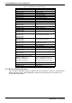
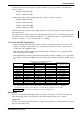
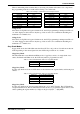
Table 2-1 Initializing the S1D13504 Registers
Operation Description
REG[1Bh] = 0x00 Enable Host Interface
REG[23h] = 0x80 Disable the Display FIFO
REG[01h] = 0x30 Set Memory Type
REG[22h] = 0x24 Set Performance Register
REG[02h] = 0x26 Set Dual/Single Panel
REG[03h] = 0x00 MOD Rate
REG[04h] = 0x4F Horizontal Display Width
REG[05h] = 0x1F Horizontal Non-Display Period
REG[06h] = 0x00 HSYNC Start Position
REG[07h] = 0x00 HSYNC Pulse Width
REG[08h] = 0xEF
REG[09h] = 0x00
Vertical Display Height
REG[0Ah] = 0x01 Vertical Non-Display Period
REG[0Bh] = 0x00 VSYNC Start Position
REG[0Ch] = 0x00 VSYNC Pulse Width
REG[0Eh] = 0xFF
REG[0Fh] = 0x03
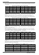
Screen 1 Line Compare
REG[10h] = 0x00
REG[11h] = 0x00
REG[12h] = 0x00
Screen 1 Display Start Address
REG[13h] = 0x00
REG[14h] = 0x00
REG[15h] = 0x00
Screen 2 Display Start Address
REG[16h] = 0xA0
REG[17h] = 0x00
Memory Address Offset
REG[18h] = 0x00 Pixel Panning
REG[19h] = 0x01 Clock Configuration
REG[1Ah] = 0x00 Power Save Configuration
REG[1Eh] = 0x00
REG[1Fh] = 0x00
General I/O Configuration
REG[20h] = 0x00
REG[21h] = 0x00
General I/O Control
REG[24h] = 0x00 Look-Up Table Address
for (index = 0; index < 16; ++index) {
REG[26h] = RED[index];
REG[26h] = GREEN[index];
REG[26h] = BLUE[index];
}
Update Look-Up Table based on the
RED[16], GREEN[16], and BLUE[16]
tables defined earlier in your program.
REG[27h] = 0x0 Look-Up Table Bank Select
REG[23h] = 0x10 Enable the Display FIFO
REG[0Dh] = 0x09 Enable Display