
User`s manual


6: TECHNICAL DESCRIPTION
S5U13504P00C REV1.0 ISA BUS EVALUATION BOARD EPSON 4-7
USER’S MANUAL (S19A-G-004-05)
6TECHNICAL DESCRIPTION
6.1 ISA Bus Support
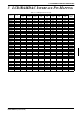
The S5U13504P00C directly supports the 16-bit ISA bus environment. All the configuration options
[MD15:0] are either hard-wired or selectable through the five-position DIP Switch S1. Refer to
Table 2-1, “Configuration DIP Switch Settings,” on page 2 for details.
Note: 1. The 8-bit ISA bus is not supported by the S5U13504P00C board design.
2. The S1D13504 is a memory-mapped device with 2M bytes of linear addressed display buffer
memory as well as a separate 37 byte register space. On the S5U13504P00C, the S1D13504
registers have been mapped to a start-address of C00000h and the 2M-byte display buffer has
been mapped to a start-address of E00000h.
3. When using this board in a PC environment, system memory must be limited to 12M bytes as
more than this will conflict with the S1D13504 display buffer/register addresses.
4. Due to backwards compatibility with the S5U13504P00C Evaluation Board, which supports both
an 8 and a 16-bit CPU interface, third party software must perform a write to address D00000h to
enable a 16-bit ISA environment. This must be done prior to initializing the S1D13504. Failure to
do so will result in the S1D13504 being configured as a 16-bit device (default, power-up), with the
ISA Bus interface (supported through the PAL (U4)) configured for an 8-bit interface.
The Epson supplied software performs this function automatically.
6.2 Non-ISA Bus Support
This evaluation board is specifically designed to support the standard 16-bit ISA bus, however, the
S1D13504 directly supports many other host bus interfaces. Header strips (H1 and H2) have been
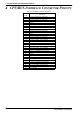
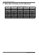
provided and contain all the necessary IO pins to interface to these buses. See Section 4, “CPU/BUS
Interface Connector Pinouts” on page 4; Table 2-1, “Configuration DIP Switch Settings,” on
page 2; and Table 2-3, “Jumper Settings,” on page 2 for details.
When using the header strips to provide the bus interface observe the following:
• All IO signals on the ISA bus card edge must be isolated from the ISA bus (do not plug the card
into a computer). Voltage lines are provided on the header strips.
• U3, a TIBPAL22V10 PAL, is currently used to provide the S1D13504 CS# (pin 4), M/R# (pin 5)
and other decode logic signals for ISA bus use. This functionality must now be provided exter-
nally; remove the PAL from its socket to eliminate conflicts resulting from two different outputs
driving the same input. Refer to Table 5-1, “Host Bus Interface Pin Mapping,” on page 6 for con-
nection details.
Note: When using a 3.3V CPU Interface, JP2 must be used to configure the S1D13504 IO VDD to 3.3V. In
this configuration all S1D13504 IO pins are configured for 3.3V output (e.g. LCD interface, DRAM in-
terface, RAMDAC interface, etc.). Although the DRAM and RAMDAC devices are 5.0V parts, they
only require a TTL V
IH of 2.4V, therefore they will operate correctly with the CMOS level output drive
of the S1D13504.
6.3 DRAM Support
The S1D13504 supports 256K x 16 as well as 1M x 16 DRAM (FPM and EDO) in symmetrical and
asymmetrical formats.
The S5U13504P00C board supports 5.0V 1M x 16 EDO DRAM (42-pin SOJ package) in symmetri-
cal format, providing a 2M byte display buffer.