
User`s manual
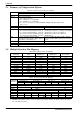

5: PIN OUT
1-10 EPSON S1D13504 SERIES HARDWARE FUNCTIONAL
SPECIFICATION (X19A-A-002-17)
5.4 Pin Description
Key:
5.4.1 Host Interface
I = Input
O = Output
I/O = Bi-Directional (Input/Output)
P = Power pin
C = CMOS level input
CD = CMOS level input with pull-down resistor
(typical values of 100KΩ/180KΩ at 5V/3.3V respectively)
CS = CMOS level Schmitt input
COx = CMOS output driver, x denotes driver type (1=3/-1.5mA, 2=6/-3mA, 3=12/-6mA)
TSx = Tri-state CMOS output driver, x denotes driver type
(1=3/-1.5mA, 2=6/-3mA, 3=12/-6mA)
TSxD = Tri-state CMOS output driver with pull-down resistor (typical values of 100KΩ/180KΩ
at 5V/3.3V respectively), x denotes driver type (1=3/-1.5mA, 2=6/-3mA, 3=12/-6mA)
CNx = CMOS low-noise output driver, x denotes driver type
(1=3/-1.5mA, 2=6/-3mA, 3=12/-6mA)
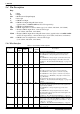
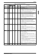
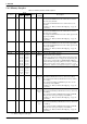
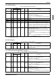
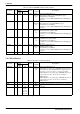
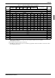
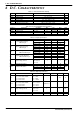
Table 5-1 Host Interface Pin Descriptions
Pin Names Type
Pin #
Driver
Reset
= 0 Value
DescriptionF00A,
F01A
F02A
AB0 I 3 5 CS Hi-Z This pin has multiple functions.
• For SH-3 mode, this pin inputs system address bit 0 (A0).
• For MC68K Bus 1, this pin inputs the lower data strobe
(LDS#).
• For MC68K Bus 2, this pin inputs system address bit 0 (A0).
• For Generic Bus, this pin inputs system address bit 0 (A0).
See Table 5-9, “Host Bus Interface Pin Mapping,” on page 16 for
summary.
AB[20:1] I 111–128
1, 2
125–142
3, 4
C Hi-Z System address bus bits [20:1].
DB[15:0] I/O 16–31 18–33 C/TS2 Hi-Z System data bus. Unused data pins should be connected to IO
V
DD.
• For SH-3 mode, these pins are connected to D[15:0].
• For MC68K Bus 1, these pins are connected to D[15:0].
• For MC68K Bus 2, these pins are connected to D[31:16] for
32-bit devices (e.g. MC68030) or D[15:0] for 16-bit devices
(e.g. MC68340).
• For Generic Bus, these pins are connected to D[15:0].
See Table 5-9, “Host Bus Interface Pin Mapping,” on page 16 for
summary.
WE1# I 9 11 CS Hi-Z This pin has multiple functions.
• For SH-3 mode, this pin inputs the write enable signal for the
upper data byte (WE1#).
• For MC68K Bus 1, this pin inputs the upper data strobe
(UDS#).
• For MC68K Bus 2, this pin inputs the data strobe (DS#).
• For Generic Bus, this pin inputs the write enable signal for the
upper data byte (WE1#).
See Table 5-9, “Host Bus Interface Pin Mapping,” on page 16.
M/R# I 5 7 C Hi-Z This input pin is used to select between the memory and register
address spaces of the S1D13504. M/R# is set high to access the
memory and low to access the registers. See Section 8.1, “Regis-
ter Mapping” on page 64.
See Table 5-9, “Host Bus Interface Pin Mapping,” on page 16.
CS# I 4 6 C Hi-Z Chip select input. See Table 5-9, “Host Bus Interface Pin Map-
ping,” on page 16.