
User`s manual


3: INTERFACING TO THE PC CARD BUS
APPLICATION NOTES (S19A-G-005-05) EPSON 5-17
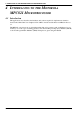
3.4 PC Card to S1D13504 Interface
3.4.1 Hardware Description
The S1D13504 is interfaced to the PC Card bus with a minimal amount of glue logic. A PAL is used
to decode the write and read signals of the PC Card bus which generate RD#, RD/WR#, WE0#,
WE1#, and CS# for the S1D13504. The also PAL inverts the reset signal of the PC card since it is
active high and the S1D13504 uses an active low reset. For PAL equations for this implementation
refer to Section 3.4.3, “PAL Equations” on page 18.
In this implementation, the address inputs (AB[20:0]) and data bus (DB[15:0] connect directly to the
CPU address (A[20:0]) and data bus (D[15:0]). M/R# is treated as an address line so that it can be
controlled using system address A21.
The PC Card interface does not provide a bus clock, so one must be supplied for the S1D13504.
Since the bus clock frequency is not critical, nor does it have to be synchronous to the bus signals, it
may be the same as CLKI.
BS# (bus start) is not used and should be tied low (connected to GND).
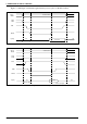
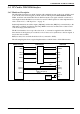
The following diagram shows a typical implementation of the PC Card to S1D13504 interface.
Figure 3-3 Typical Implementation of PC Card to S1D13504 Interface
OE#
WE#
CE1#
CE2#
REG#
RESET
A[21:0]
D[15:0]
WAIT#
RD#
RD/WR#
WE0#
WE1#
CS#
RESET#
M/R#
AB[20:0]
DB[15:0]
WAIT#
BUSCLK
CLKI
PC Card socket PAL16L8-10 S1D13504
A21
15K pull-up
Oscillator