
User`s manual


4: INTERFACING TO THE MOTOROLA MPC821 MICROPROCESSOR
5-24 EPSON APPLICATION NOTES (S19A-G-005-05)
Normal (Non-Burst) Bus Transactions
A data transfer is initiated by the bus master by placing the memory address on address lines A0
through A31 and driving TS (Transfer Start) low for one clock cycle. Several control signals are also
provided with the memory address:
• TSIZ[0:1] (Transfer Size), which indicate whether the bus cycle is 8, 16, or 32 bits in width.
• RD/WR, which is high for read cycles and low for write cycles.
• A set of address type signals (AT[0:3]) which provide more detail on the type of transfer being
attempted.
When the peripheral device being accessed has completed the bus transfer, it asserts TA (Transfer
Acknowledge) for one clock cycle, completing the bus transaction. Once TA has been asserted, the
MPC821 will not start another bus cycle until TA has been de-asserted. The minimum length of a
bus transaction is two bus clocks.
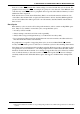
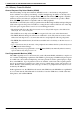
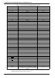
Figure 4-1 illustrates a typical memory read cycle on the Power PC system bus, and Figure 4-2 illus-
trates a memory write cycle.
Figure 4-1 Power PC Memory Read Cycle
Figure 4-2 Power PC Memory Write Cycle
A[0:31]
D[0:31]
TSIZ[0:1], AT[0:3]
TS
TA
SYSCLK
Wait StatesTransfer Start Transfer Next Transfer
Sampled when TA low
RD/WR
Complete Starts
A[0:31]
D[0:31]
TSIZ[0:1], AT[0:3]
TS
TA
SYSCLK
Wait StatesTransfer Start
RD/WR
Valid
Transfer Next Transfer
Complete Starts