
User`s manual


5: INTERFACING TO THE MOTOROLA MCF5307 MICROPROCESSOR
5-36 EPSON APPLICATION NOTES (S19A-G-005-05)
5.2 Interfacing to the MCF5307
5.2.1 The MCF5307 System Bus
The MCF5200/5300 family of processors feature a high-speed synchronous system bus typical of
modern microprocessors. This section is an overview of the operation of the CPU bus to establish
interface requirements.
5.2.2 Overview
The MCF5307 microprocessor family uses a synchronous address and data bus, very similar in
architecture to the MC68040 and MPC8xx. All outputs and inputs are timed with respect to a
square-wave reference clock called BCLK0 (Master Clock). This clock runs at a software-selectable
divisor rate from the machine cycle speed of the CPU core, typically 20 to 33 MHz. Both the address
and the data bus are 32 bits in width. All IO accesses are memory-mapped; there is no separate IO
space in the Coldfire architecture.
The bus can support two types of cycle, normal and burst. Burst memory cycles are used to fill on-
chip cache memories, and for certain on-chip DMA operations. Normal cycles are used for all other
data transfers.
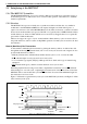
Normal (Non-Burst) Bus Transactions
A data transfer is initiated by the bus master by placing the memory address on address lines A31
through A0 and driving TS (Transfer Start) low for one clock cycle. Several control signals are also
provided with the memory address:
• SIZ[1:0] (Transfer Size), which indicate whether the bus cycle is 8, 16, or 32 bits in width.
• R/W, which is high for read cycles and low for write cycles.
• A set of transfer type signals (TT[1:0]) which provide more detail on the type of transfer being
attempted.
• TIP (Transfer In Progress), which is asserted whenever a bus cycle is active.
When the peripheral device being accessed has completed the bus transfer, it asserts TA (Transfer
Acknowledge) for one clock cycle, completing the bus transaction. Once TA has been asserted, the
MCF5307 will not start another bus cycle until TA has been de-asserted. The minimum length of a
bus transaction is two bus clocks.
Figure 5-1 illustrates a typical memory read cycle on the MCF5307 system bus, and Figure 5-2 illus-
trates a memory write cycle.
Figure 5-1 MCF5307 Memory Read Cycle
A[31:0]
D[31:0]
SIZ[1:0], TT[1:0]
TS
TA
BCLK0
Wait StatesTransfer Start Transfer Next Transfer
Sampled when T
A low
R/W
Complete Starts
TIP