
User`s manual


5: INTERFACING TO THE MOTOROLA MCF5307 MICROPROCESSOR
5-40 EPSON APPLICATION NOTES (S19A-G-005-05)
5.4 MCF5307 To S1D13504 Interface
5.4.1 Hardware Connections
The S1D13504 requires a 2M byte address space for the display buffer RAM, plus a few more loca-
tions to access its internal registers. Chip selects 0 and 1 have programmable block sizes from 64K
bytes through 2G bytes, however these chip selects would normally be needed to control system
RAM and ROM. Two of the I/O chip selects (CS2 through CS7) are required to address the entire
address space of the S1D13504, since these chip selects have a fixed 2M byte block size.
Since the S1D13504 has a single chip select input for both display RAM and registers, a single
external gate is required to produce a negative-OR function of the two MCF5307 chip selects. A sin-
gle resistor is used to speed up the rise time of the WAIT# (TA) signal when terminating the bus
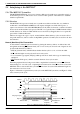
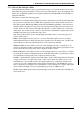
cycle. Figure 5-3 shows a block diagram of the interface.
Figure 5-3 Block Diagram of MCF5307 to S1D13504 Interface
A21
A[20:0]
D[31:15]
CS4
CS5
TA
WE0
WE1
OE
BCLK0
RESET
M/R#
AB[20:0]
SD[15:0]
CS#
WAIT#
WE1#
WE0#
RD1#
RD0#
BUSCLK
RESET#
MCF5307 S1D13504
Vcc
470 pull-up
74AC08 (or equivalent)