
User`s manual


5: INTERFACING TO THE MOTOROLA MCF5307 MICROPROCESSOR
5-42 EPSON APPLICATION NOTES (S19A-G-005-05)
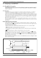
5.4.3 MCF5307 Chip Select Configuration
In the example interface, chip selects 4 and 5 are used to control the S1D13504. CS4 selects a 2M
byte address space for the S1D13504’s control registers, while CS5 selects the 2M byte display
RAM buffer. The CSBAR register should be set to the upper 8 bits of the desired base address.
The following options should be selected in the chip select mask registers (CSMR4/5):
• WP = 0 – disable write protect
• AM = 0 – enable alternate bus master access to the S1D13504
• C/I = 1 – disable CPU space access to the S1D13504
• SC = 1 – disable Supervisor Code space access to the S1D13504
• SD = 0 – enable Supervisor Data space access to the S1D13504
• UC = 1 – disable User Code space access to the S1D13504
• UD = 0 – enable User Data space access to the S1D13504
• V = 1 – global enable (“Valid”) for the chip select
The following options should be selected in the chip select control registers (CSCR4/5):
• WS0–3 = 0 – no internal wait state setting
• AA = 0 – no automatic acknowledgment
• PS (1:0) = 1:0 – memory port size is 16 bits
• BEM = 0 – Byte enable/write enable active on writes only
• BSTR = 0 – disable burst reads
• BSTW = 0 – disable burst writes