
User`s manual


5: PIN OUT
1-16 EPSON S1D13504 SERIES HARDWARE FUNCTIONAL
SPECIFICATION (X19A-A-002-17)
5.5 Summary of Configuration Options
5.6 Multiple Function Pin Mapping
*1: All GPIO pins default to input on reset, and unless programmed otherwise should be connected to either
V
SS or IO VDD if not used.
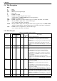
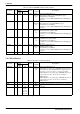
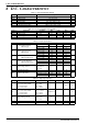
Table 5-8 Summary of Power On / Reset Options
Pin Name
Value on this pin at rising edge of RESET# is used to configure: (1/0)
1 0
MD0 8-bit host bus interface 16-bit host bus interface
MD[3:1] Select host bus interface:
000 = SH-3 bus interface
001 = MC68K bus 1 (e.g. MC68000)
010 = MC68K bus 2 (e.g. MC68030)
011 = Generic bus interface (e.g. Philips MIPS PR31500/PR31700; NEC MIPS VR4102)
1XX = reserved
MD4 Little Endian Big Endian
MD5 WAIT# is active high (1 = insert wait state) WAIT# is active low (0 = insert wait state)
MD[7:6] Memory Address/GPIO configuration:
00 = symmetrical 256K×16 DRAM. MA[8:0] = DRAM address. MA[11:9] = GPIO[2:1] and GPIO3
01 = symmetrical 1M×16 DRAM. MA[9:0] = DRAM address. MA[11:10] = GPIO[2:1]
10 = asymmetrical 256K×16 DRAM. MA[9:0] = DRAM address. MA[11:10] = GPIO[2:1]
11 = asymmetrical 1M×16 DRAM. MA[11:0] = DRAM address.
MD8 Configure DACRD#, BLANK#, DACP0,
DACWR#, DACRS0, DACRS1, HRTC, VRTC as
General Purpose IO (GPIO[11:4]).
Configure DACRD#, BLANK#, DACP0, DACWR#,
DACRS0, DACRS1, HRTC, VRTC as DAC and CRT
outputs.
MD9 SUSPEND# pin configured as GPO output. SUSPEND# pin configured as SUSPEND# input.
MD10 Active low LCDPWR or GPO polarities. Active high LCDPWR or GPO polarities.
MD[15:11] Not used.
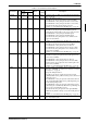
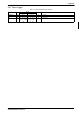
Table 5-9 Host Bus Interface Pin Mapping
S1D13504
Pin Names
SH-3 MC68K Bus 1 MC68K Bus 2 Generic MPU
AB[20:1] A[20:1] A[20:1] A[20:1] A[20:1]
AB0 A0 LDS# A0 A0
DB[15:0] D[15:0] D[15:0] D[31:16] D[15:0]
WE1# WE1# UDS# DS# WE1#
M/R# External Decode External Decode External Decode External Decode
CS# CSn# External Decode External Decode External Decode
BUSCLK CKIO CLK CLK BCLK
BS# BS# AS# AS# Connect to IO V
DD
RD/WR# RD/WR# R/W# R/W# RD1#
RD# RD# Connect to IO VDD SIZ1 RD0#
WE0# WE0# Connect to IO VDD SIZ0 WE0#
WAIT# WAIT# DTACK# DSACK1# WAIT#
RESET# RESET# RESET# RESET# RESET#
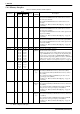
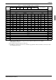
Table 5-10 Memory Interface Pin Mapping
S1D13504
Pin Names
FPM/EDO-DRAM
Sym 256K × 16 Asym 256K × 16 Sym 1M × 16 Asym 1M × 16
2CAS# 2WE# 2CAS# 2WE# 2CAS# 2WE# 2CAS# 2WE#
MD[15:0] DQ[15:0]
MA[8:0] A[8:0]
MA9
GPIO3
∗1
A9
MA10
GPIO1
∗1
A10
MA11
GPIO2
∗1
A11
UCAS# UCAS# UWE# UCAS# UWE# UCAS# UWE# UCAS# UWE#
LCAS# LCAS# CAS# LCAS# CAS# LCAS# CAS# LCAS# CAS#
WE# WE# LWE# WE# LWE# WE# LWE# WE# LWE#
RAS# RAS#