
User`s manual


7: A.C. CHARACTERISTICS
1-20 EPSON S1D13504 SERIES HARDWARE FUNCTIONAL
SPECIFICATION (X19A-A-002-17)
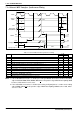
7.1 CPU Interface Timing
7.1.1 SH-3 Interface Timing
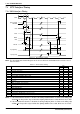
Figure 7-1 SH-3 Interface Timing
Note: The SH-3 Wait State Control Register for the area in which the S1D13504 resides must be set to a
non-zero value.
Note: 1.
If the S1D13504 host interface is disabled, the timing for WAIT# driven is relative to the falling edge
of CSn# or
the first positive edge of CKIO after A[20:0], M/R# becomes valid, whichever one is later.
2.
If the S1D13504 host interface is disabled, the timing for D[15:0] driven is relative to the falling edge
of RD# or
the first positive edge of CKIO after A[20:0], M/R# becomes valid, whichever one is later.
Table 7-1 SH-3 Interface Timing
Symbol Parameter
3.3V
Units
Min. Max.
t1
Clock period 25 ns
t2
Clock pulse width high 5 ns
t3
Clock pulse width low 5 ns
t4
A[20:0], M/R#, RD/WR# setup to CKIO 4 ns
t5
A[20:0], M/R#, RD/WR# hold from CS# 0 ns
t6
BS# setup 3ns
t7
BS# hold 0ns
t8
CSn# setup 0ns
t9
2
Falling edge RD# to D[15:0] driven 3 ns
t10
Rising edge CSn# to WAIT# tri-state 0 4 ns
t11
Falling edge CSn# to WAIT# driven 1 11 ns
t12
CKIO to WAIT# delay 3 15 ns
t13
D[15:0] setup to first CKIO after BS# (write cycle) 0 ns
t14
D[15:0] hold (write cycle) 0 ns
t15
D[15:0] valid to WAIT# rising edge (read cycle) 0 ns
t16
Rising edge RD# to D[15:0] tri-state (read cycle) 2 9 ns
t1 t2 t3
t4
t10
t11
t15
t5
t6 t7
t8
t9
t12
t16
t13
t14
CKIO
A[20:0], M/R#
CSn#
RD/WR#
RD#
D[15:0](read)
BS#
WAIT#
WEn#
D[15:0](write)
t12