
User`s manual


7: A.C. CHARACTERISTICS
S1D13504 SERIES HARDWARE FUNCTIONAL EPSON 1-35
SPECIFICATION (X19A-A-002-17)
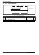
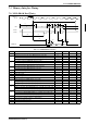
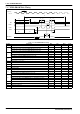
7.3.6 FPM-DRAM Read Timing
Figure 7-17 FPM-DRAM Read Timing
Table 7-17 FPM DRAM Read Timing
Symbol Parameter Min. Typ. Max. Units
t1
Memory clock
40 ns
t2
Random read or write cycle time (REG[22h] bits [6:5] = 00)
5
t1
ns
Random read or write cycle time (REG[22h] bits [6:5] = 01)
4
t1
ns
Random read or write cycle time (REG[22h] bits [6:5] = 10)
3
t1
ns
t3
Row address setup time (REG[22h] bits [3:2] = 00)
2
t1
ns
Row address setup time (REG[22h] bits [3:2] = 01)
1.45
t1
ns
Row address setup time (REG[22h] bits [3:2] = 10)
1
t1
ns
t4
Row address hold time (REG[22h] bits [3:2] = 00 or 10)
t1 - 1
ns
Row address hold time (REG[22h] bits [3:2] = 01)
0.45 t1 - 1
ns
t5
Column address setup time
0.45
t1 - 1
ns
t6
Column address hold time
0.45
t1 - 1
ns
t7
CAS# pulse width
0.45
t1 0.55 t1 + 1
ns
t8
CAS# precharge time
0.45
t1 - 1 0.55 t1
ns
t9
RAS# hold time
0.45
t1
ns
t10
RAS# precharge time (REG[22h] bits [3:2] = 00)
2
t1 - 1
ns
RAS# precharge time (REG[22h] bits [3:2] = 01)
1.45 t1 - 1
ns
RAS# precharge time (REG[22h] bits [3:2] = 10)
1 t1 - 1
ns
t11
RAS# to CAS# delay time (REG[22h] bit 4 = 1 and bits [3:2] = 00 or 10)
1.45
t1 - 2 1.55 t1
ns
RAS# to CAS# delay time (REG[22h] bit 4 = 0 and bits [3:2] = 00 or 10)
2.45
t1 - 2 2.55 t1
ns
RAS# to CAS# delay time (REG[22h] bit 4 = 1 and bits [3:2] = 01)
1
t1 - 2 1 t1
ns
RAS# to CAS# delay time (REG[22h] bit 4 = 0 and bits [3:2] = 01)
2
t1 - 2 2 t1
ns
t12
Access time from RAS# (REG[22h] bit 4 = 1 and bits [3:2] = 00 or 10)
2
t1 - 2
ns
Access time from RAS# (REG[22h] bit 4 = 0 and bits [3:2] = 00 or 10)
3 t1 - 2
ns
Access time from RAS# (REG[22h] bit 4 = 1 and bits [3:2] = 01)
1.45
t1 - 2
ns
Access time from RAS# (REG[22h] bit 4 = 0 and bits [3:2] = 01)
2.45
t1 - 2
ns
t13
Access time from CAS#
0.45
t1 - 1
ns
t14
Access time from CAS# precharge
1
t1 - 2
ns
t15
Read Data hold from CAS# or RAS#
2ns
d1
d2
RAS#
CAS#
MA
MD(Read)
t10
t12
t13
t15
R
C1
C4
t3 t4
t6t5
t7
t8
t11
t9
d3
d4
t14
t2
t1
C2 C3
Memory
Clock