
User`s manual


8: REGISTERS
S1D13504 SERIES HARDWARE FUNCTIONAL EPSON 1-71
SPECIFICATION (X19A-A-002-17)
bit 1 CRT Enable
This bit enables the CRT control signals.
Note: REG[02h] bit 1 must = 0 when in CRT only mode.
bit 0 LCD Enable
This bit enables the LCD control signals. Programming this bit from a 0 to a 1 starts the
LCD power-on sequence. Programming this bit from a 1 to a 0 starts the LCD power-off
sequence.
REG[0Eh] bits 7–0, REG[0Fh] bits 1–0
Screen 1 Line Compare Bits [9:0]
In split screen mode, the panel is divided into screen 1 and screen 2, with screen 1 above
screen 2. This is the 10-bit value that specifies the screen 1 size in 1-line resolution for
split screen mode.
Split screen 1 vertical size in number of lines = (ContentsOfThisRegister) + 1.
Where ContentsOfThisRegister is a 10-bit value comprising of these registers. The maxi-
mum screen 1 vertical size is 1024 lines. Screen 2 is visible only if the screen 1 line com-
pare is less than the vertical panel size. The starting address for screen 1 is given by the
Screen 1 Display Start Address registers. The starting address for screen 2 is given by the
Screen 2 Display Start Address registers. See Section 10.2, “Image Manipulation” on
page 90 and “S1D13504 Programming Notes and Examples”, document number S19A-
G-002-xx, Section 4 for more details.
Note: For normal operation (no split screen) this register must be set greater than the vertical
display height REG[08h] and REG[09h] (e.g. set to 3FFh).
REG[10h] bits 7–0, REG[11h] bits 7–0, REG[12h] bits 3–0
Screen 1 Start Address Bits [19:0]
This register forms the 20-bit address for the starting word of the screen 1 image in the
display buffer. Note that this is a word address. An entry of 0000h into these registers rep-
resents the first word of display memory, an entry of 0001h represents the second word of
display memory, and so on. See Section 10, “Display Configuration” on page 88 for
details.
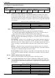
Screen 1 Line Compare Register 0
REG[0Eh] RW
Screen 1 Line
Compare Bit 7
Screen 1 Line
Compare Bit 6
Screen 1 Line
Compare Bit 5
Screen 1 Line
Compare Bit 4
Screen 1 Line
Compare Bit 3
Screen 1 Line
Compare Bit 2
Screen 1 Line
Compare Bit 1
Screen 1 Line
Compare Bit 0
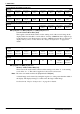
Screen 1 Line Compare Register 1
REG[0Fh] RW
n/a n/a n/a n/a n/a n/a
Screen 1 Line
Compare Bit 9
Screen 1 Line
Compare Bit 8
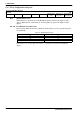
Screen 1 Display Start Address Register 0
REG[10h] RW
Start Address
Bit 7
Start Address
Bit 6
Start Address
Bit 5
Start Address
Bit 4
Start Address
Bit 3
Start Address
Bit 2
Start Address
Bit 1
Start Address
Bit 0
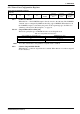
Screen 1 Display Start Address Register 1
REG[11h] RW
Start Address
Bit 15
Start Address
Bit 14
Start Address
Bit 13
Start Address
Bit 12
Start Address
Bit 11
Start Address
Bit 10
Start Address
Bit 9
Start Address
Bit 8
Screen 1 Display Start Address Register 2
REG[12h] RW
n/a n/a n/a n/a
Start Address
Bit 19
Start Address
Bit 18
Start Address
Bit 17
Start Address
Bit 16