
User`s manual


8: REGISTERS
1-74 EPSON S1D13504 SERIES HARDWARE FUNCTIONAL
SPECIFICATION (X19A-A-002-17)
8.2.5 Clock Configuration Register
bit 2 MCLK Divide Select
When this bit = 1 the memory clock (MCLK) frequency is half of the input clock fre-
quency. When this bit = 0 the memory clock frequency is equal to the input clock fre-
quency.
bits 1–0 PCLK Divide Select Bits [1:0]
These bits determine the amount of divide from the memory clock to generate the pixel
clock (PCLK):
See Section 11.2, “Frame Rate Calculation” on page 92 for selection of PCLK fre-
quency.
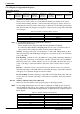
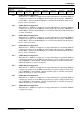
Clock Configuration Register
REG[19h] RW
n/a n/a n/a n/a n/a
MCLK Divide
Select
PCLK Divide
Select Bit 1
PCLK Divide
Select Bit 0
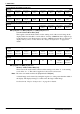
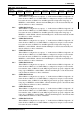
Table 8-9 PCLK Divide Selection
PCLK Divide Select Bits [1:0] MCLK/PCLK Frequency Ratio
00 1:1
01 2:1
10 3:1
11 4:1