
User`s manual


8: REGISTERS
S1D13504 SERIES HARDWARE FUNCTIONAL EPSON 1-81
SPECIFICATION (X19A-A-002-17)
Note: Changing this register to non-zero value, or to a different non-zero value, should be done
only when there are no read/write DRAM cycles. This condition occurs when both the Dis-
play FIFO is disabled (REG[23h] bit 7 = 1) and the Half Frame Buffer is disabled
(REG[1Bh] bit 0 = 1). For programming information, see “S1D13504 Programming Notes
and Examples”, document number S19A-G-002-xx.
bit 7 EDO Read-Write Delay
This bit is used for EDO-DRAM to select the delay during the read-write transition. A “0”
selects 2 MCLK delay for the read-write transition. A “1” selects 1 MCLK delay for the
read-write DRAM. This bit has no effect for FPM-DRAM which always uses 1 MCLK
delay for the read-write transition. This bit may be programmed to 1 when the MCLK fre-
quency is less than 30MHz.
bits 6–5 RC Timing Value (NRC) Bits [1:0]
These bits select the DRAM random-cycle timing parameter, tRC. These bits specify the
number (NRC) of MCLK periods (TM) used to create tRC. NRC should be chosen to meet
tRC as well as tRAS, the RAS pulse width. Use the following two formulae to calculate
NRC then choose the larger value. Note, these formulae assume an MCLK duty cycle of
50 ± 5%.
NRC = Round-Up (tRC/TM)
NRC = Round-Up (tRAS/TM + NRP) if NRP = 1 or 2
= Round-Up (tRAS/TM + 1.55) if NRP = 1.5
The resulting tRC is related to NRC as follows:
tRC = (NRC) TM
bit 4 RAS# to CAS# Delay (NRCD)
This bit selects the DRAM RAS# to CAS# delay parameter, tRCD. This bit specifies the
number (NRCD) of MCLK periods (TM) used to create tRCD. NRCD must be chosen to sat-
isfy the RAS# access time, tRAC. Note, these formulae assume an MCLK duty cycle of 50
± 5%.
NRCD = Round-Up ((tRAC + 5)/TM - 1) if EDO and NRP = 1 or 2
= 2 if EDO and NRP = 1.5
= Round-Up (tRAC/TM - 1) if FPM and NRP = 1 or 2
= Round-Up (tRAC/TM - 0.45) if FPM and NRP = 1.5
Note that for EDO-DRAM and NRP = 1.5, this bit is automatically forced to 0 to select 2
MCLK for NRCD. This is done to satisfy the CAS# address setup time, tASC.
The resulting tRCD is related to NRCD as follows:
tRCD = (NRCD) TM if EDO and NRP = 1 or 2
tRCD = (1.5) TM if EDO and NRP = 1.5
tRCD = (NRCD + 0.5) TM if FPM and NRP = 1 or 2
tRCD = (NRCD) TM if FPM and NRP = 1.5
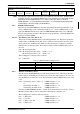
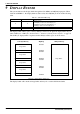
Performance Enhancement Register 0
REG[22h] RW
EDO Read-
Write Delay
RC Timing
Value Bit 1
RC Timing
Value Bit 0
RAS# to CAS#
Delay
RAS#
Precharge
Timing Bit 1
RAS#
Precharge
Timing Bit 0
n/a Reserved
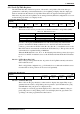
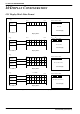
Table 8-11 Minimum Memory Timing Selection
REG[22h] Bits [6:5] N
RC Minimum Random Cycle Width (tRC)
00 5 5 TM
01 4 4 TM
10 3 3 TM
11 Reserved Reserved