
Power Supply User Manual

S1F76300 Series
S1F70000 Series EPSON 4–21
Technical Manual
S1F76300
Series
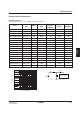
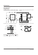
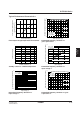
Output voltage adjustment
To ensure stable output, any circuit that adjusts the out-
put voltage must contain C1, R
A and RB. To stop
switching current from affecting V
O, the circuit must
also satisfy the condition I
O < IR.
The following figure summarizes the relevant circuits
inside an S1F76300 series chip.
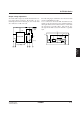
V
O is connected to the level shift and buffer circuit,
which provide the gate bias for the switching transistor
driving the inductor. The current drain, I
O1, varies with
the load and is typically 10µA. The current, I
O2,
through the internal resistors R1 and R2, is typically
1µA.
V
I
V
O
I
O
C
L
(I
O
< I
R
)
I
R
R
B
R
A
C
GND
V
SW
Voltage adjustment
circuit
Step-up
voltage
output
S1F76310M
V
SW
V
I
Comparatpr
Controller
Level
shifter
V
O
I
O1
I
O2
V
REF
R1
R2
I
O
Buffer