
Power Supply User Manual


6–2EPSONS1F70000 Series
Technical Manual
Appendix
Symbol Parameter
I
OPR2 Stabilization circuit power dissipation
I
Q Quiescent current
I
R Reverse current
I
SWQ Switching transistor leakage current
K
I Output voltage temperature gradient
P
D Power dissipation
P
eff Voltage multiplication efficiency
R
BSON Backup switch ON resistance
R
L Load resistance
R
O Output impedance
R
ON ON resistance
R
OSC Oscillator network resistor
R
RV Stabilization voltage sensing resistor
R
RVn Reference voltage
R
SAT Stabilization output saturation resistance
R
SWON Switching transistor ON resistance
T
a Ambient temperature
t
AE Minimum pulsewidth
t
HA Address hold time
t
HD Data hold time
THD Total harmonic distortion
θ
jn Thermal resistance
t
MRR Memory reset recovery time
Symbol Parameter
C
D Drain capacitance
C
F8 Field slew capacitance
C
G Gate capacitance
C
I Input capacitance
C
n Capacitance
CT Crosstalk
C
Tn Temperature gradient
f
CLK Clock frequency
f
max Maximum clock frequency
f
OSC Oscillator frequency
FT Field through (channel OFF)
I
BSQ Backup switching leakage current
I
DDO Operating current
I
DDS Standby current
I
DD Power supply current
I
IH High-level input current
I
IL Low-level input current
I
LKI input leakage current
I
MAX Maximum current
I
O Output current
I
OH High-level output current
I
OL Low-level output current
I
OPR1 Multiplier circuit power dissipation
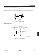
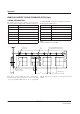
The following figure shows a thermal design
model which can be used to determine heatsink
capacity.
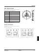
2. Ensure that the regulator common pin is a sin-
gle-point ground to prevent earth loops. Make
ground lines as thick and short as possible. Use the
specified bypass capacitors for inputs and outputs.
If there is a switching load, use a tantalum or
ceramic capacitor, as these devices have a high
frequency response between the power supply and
ground.
Junction
temperature
Case
temperature
Heatsink
temperature
Ambient
temperature
Heat
source
T
j
T
c
T
s
T
a
θ
jc
θ
cs
θ
sa
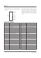
PARAMETER SUMMARY