
Power Supply User Manual


S1F76540 Series
2–24 EPSON S1F70000 Series
Technical Manual
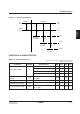
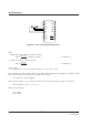
Voltage Converter
The voltage converter, consisting of a boost control cir-
cuit and a voltage converter circuit, receives clocks
from the clock generator circuit and boosts the input
power voltage (V
I) four, three or two times. During
four-time boosting, however, the three-time and two-
time boost outputs cannot be obtained simultaneously.
Figure 2.4 gives the potential relationship during four-,
three- and two-time boosting. The C2P pin is also used
as the master clock output during parallel connection.
Figure 2.4 Electrical potentials during boosting (at –5V input)
Caution:
• When connecting a capacitor to the C1P, C2P, C1N, C2N, C3N, or V
O pin for voltage conversion,
close the capacitor to the IC package as much as possible to minimize the wiring length.
V
DD
(0 V)
V
I
(–5 V)
10 V
15 V
20 V
–10 V
–15 V
–20 V
Two-time
boosting
Three-time
boosting
Four-time
boosting