
Power Supply User Manual


S1F76540 Series
S1F70000 Series EPSON 2–31
Technical Manual
S1F76540
Series
◊
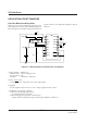
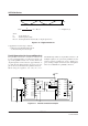
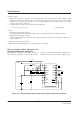
Setup conditions of Figure 2.9
• Internal clock : ON (Low Output mode)
• Booster circuit : ON
• Regulator : OFF
◊
Power-off procedure
• Set the P
OFF2 pin to low (VI) to turn off all circuits.
◊
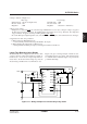
Ripple voltage
• As the output at V
O pin is unstable, it can contain ripple components as shown in Figure 2.10. The ripple voltage
(V
RP) increases according to the load current, and it can roughly be calculated by equation (4).
Figure 2.9 Wiring example of 4-time booster
V
O
V
RI
V
REG
RV
V
DD
FC
TC1
TC2
C2P
C2N
C3N
C1N
C1P
V
I
P
OFF1
P
OFF2
C2
C1
C3
1
2
3
4
5
6
7
8
C
I
V
I
V
DD
V
O
C
O
+
+
+
16
15
14
13
12
11
10
9
+
+
4-time Booster
Only the booster circuit operates, and it boosts the input
voltage (V
I) four times in negative direction and outputs
it at the V
O pin. As the regulator is not used, the voltage
appearing at the V
O pin may contain ripple components.
Figure 2.9 gives a wiring example.