
Specifications


SCI7910Y Series
SCI7000 Series EPSON 3–29
Technical Manual
Voltage
Regulator
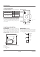
Differential amplifier
The built-in differential amplifier generates a potential
at point X that adjusts the gate bias of the output transis-
tor if there is any difference betweeen V
REF and VREG.
V
REG
To output
transistor
V
SS
V
REF
V
I
N1 N2
P1 P2
X
Output transistor
The output side of the p-channel MOS transistors in the
output transistor circuit is connected to the voltage di-
vider resistors in the feedback loop.
R
1
V
REG
V
REF
{
|
V
1
V
O
V
SS
R
2
TYPICAL APPLICATIONS
Current Booster
At the cost of a small increase in current consumption,
the voltage is regulated while maintaining high current
output.
GND
VO
VI
V
O
V
SS
V
I
SCI7910Y
External Voltage Converter
The following circuit raises the output voltage of a
SCI7910Y series IC.
R
1
I
opr
GND
V
O
V
O
V
r
V
I
V
I
V
SS
R
2
I
B
SCI7910Y
The following equation shows the relationship between
the old and new voltages.
R1 + R2
VO =—————VR
R2
Note that the application must supply a bias current, IB,
high enough to offset the increase in voltage across R
1
due to Iopr.
An alternative circuit for raising the output voltage is
shown in the following figure.
VO
VI
R1COCI
GND
VI
ISS
VO
VSS
SCI7910Y
This configuration, however, introduces two design
problems.
1. It reduces the output voltage by V
F, the forward volt-
age drop across the diode.
2. It is sensitive to fluctuations in V
F due to differences
in diodes, operating temperatures and I
SS.