7.
SED1560 Series Contents OVERVIEW .......................................................................................................................................................... 7-1 FEATURES ........................................................................................................................................................... 7-1 PAD LAYOUT ...........................................................................................................................................
SED1560 Series FR Control Circuit ...................................................................................................................................... 7-32 Power Supply Circuit .................................................................................................................................. 7-32 Voltage Tripler ............................................................................................................................................ 7-33 Voltage Regulator .
SED1560 Series OVERVIEW The SED1560 series is a single-chip LCD driver for dotmatrix liquid crystal displays. It accepts serial or 8-bit parallel display data directly from a microprocessor and stores data in an on-chip 166 × 65-bit RAM.
SED1560 Series V5 V4 V3 V2 V1 VDD VR V5 VOUT CAP2– CAP2+ CAP1– CAP1+ VSS T1 T2 OSC1 OSC2 CL FR SYNC CLO DYO D7 D6 D5 D4 D3 D2 D1 D0 VSS RD WR A0 C86 CS2 CS1 P/S S1 SCL RES M/S VDD V1 V2 V3 V4 V5 PAD LAYOUT O0 1 216 49 COM1 O165 D156✻D 0B 95 8.08 × 5.28 mm 100 µm (Min.) 625 µm 300 µm (Al-pad) Chip size Pad pitch Chip thickness : : : : Bump size A : 103 µm × 95 µm (Typ.) (Pad No. 1 ~ 6, 18, 36 ~ 42, 44 ~ 49) : 69 µm × 95 µm (Typ.) (other then the above) : 23 µm (Typ.
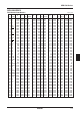
SED1560 Series SED1560SERIES Unit : µm PAD Center Coordinates PAD PIN No.
SED1560 Series BLOCK DIAGRAM O0 to O31 O32 to O101 O102 to O165 COMI VSS VDD VDD V1 V1 V2 Common and segment driver V3 V4 Common and segment driver Segment driver V2 Common I V3 V4 V5 V5 Frame control Shift register Shift register CAP1+ CAP1– CAP2+ Supply voltage generator1 166–bit display data latch CAP2– VR T1, T2 Output status select I/O buffer Line address decoder 166 x 65–bit display data RAM Line counter Display initial line register 166–bit column address decoder FR 8–bi
SED1560 Series PIN DESCRIPTION Power Supply Number of pins I/O Name Description 2 Supply VDD 5V supply. Common to MPU power supply pin VCC. 2 Supply VSS Ground 11 Supply V1 to V5 LCD driver supply voltages. The voltage determined by the LCD cell is impedance-converted by a resistive divider or an operational amplifier for application. Voltages should be determined on a VDDbasis so as to satisfy the following relationship. The voltages must satisfy the following relationship.
SED1560 Series Microprocessor Interface Number of pins I/O Name Description 8 I/O D0 to D7 1 I A0 1 I RES 2 I CS1, CS2 1 I RD (E) Read enable input. See note. 1 1 I WR (R/W) Write enable input. See note. 2 1 I C86 1 I SI 1 I SCL Serial clock input. Data is read on the rising edge of SCL and converted to 8-bit parallel data. 1 I P/S Parallel/serial data input select Data inputs/outputs Control/display data flag input.
SED1560 Series Oscillator and Timing Control Number of pins I/O Name Description 2 I OSCI Connecting pins for feedback resistors of the built-in oscillator When M/S = “H”: Connect oscillator resistor Rf to the OSC1 and OSC2 pins. The OSC2 pin is used for output of the oscillator amplifier. 2 I/O OSC2 When M/S = “L”: The OSC2 pin is used for input of oscillation signal. The OSC1 pin should be left open.
SED1560 Series LCD Driver Outputs Number of pins I/O Name Description 166 O O0 to O165 LCD driver outputs. O0 to O31 and O102 to O165 are selectable segment or common outputs, determined by a selection command. O32 to O101 are segment outputs only. For segment outputs, the ON voltage level is given as shown in the following table.
SED1560 Series SPECIFICATIONS Absolute Maximum Ratings Parameter Symbol Rating Unit Supply voltage (1) Supply voltage range (2) (DC/DC When in use) VSS –7.0 +0.03 –6.0 to 0.3 (when triple boosting) V Driver supply voltage range (1) V5 –18.0 to 0.3 V Driver supply voltage range (2) V1, V 2, V3, V4 V5 to 0.3 V Input voltage range VIN VSS –0.3 to 0.3 V Output voltage range Vo VSS –0.3 to 0.3 V Operating temperature range Topr –30 to 85 deg.
SED1560 Series DC Characteristics VDD = 0 V, VSS = –5 V ± 10%, Ta = –30 to +85°C unless otherwise noted. Item Symbol Power Recommendvoltage (1) ed operation Condition Min. Typ. Max. Unit VSS –5.5 –5.0 –4.5 V –6.0 –2.4 V5 –16.0 –4.0 V V5 *2 voltage (2) Operational V1 , V2 0.4 × V5 VDD V V1, V2 Operational V3 , V4 V5 0.6 × V5 V V3, V4 VIHC1 0.3 × V SS VDD V VIHC2 0.
SED1560 Series When dynamic current consumption (I) is displaye; the built-in power circuit is on and T1 = T2 = Low. VDD = 0 V, VSS = –5 V ± 10%, Ta = –30 to +85°C unless otherwise noted. Item Symbol Condition Min. Typ. Max. Unit SED1560 V5 = –12.5 V; 3 times amplified 169 340 µA SED1561 V5 = –8.0 V ; 3 times amplified 124 250 µA V5 = –6.0 V ; 2 times amplified 53 110 µA VSS = –2.7 V; 3 times amplified 66 130 µA SED1562 IDD (1) Remarks *16 V5 = –6.
SED1560 Series - Dynamic current consumption (I), if the built-in power supply is used. Conditions: 200 (µA) I DD 0 56 ED1 S 150 (1) 100 62 0 SED15 1 2 3 4 VDD 5 V5 – VDD = –12.5 V; 3 times amplified SED1561 V5 – VDD = –8.0 V; 3 times amplified SED1562 V5 – VDD = –6.0 V; 2 times amplified Internal oscillation: SED1560 Rf = 1 MΩ SED1561 Rf = 1 MΩ SED1562 Rf = 1 MΩ *16 SED1560 1561 SED 50 The built-in power supply is on and T1 = T2 = Low. 6 7 (V) Remarks: Notes: *1.
SED1560 Series The relationship between oscillator frequency fOSC and LCD frame frequency f F is obtained from the following expression. Oscillator frequency vs. frame vs. Rf [SED156✽D0B] Ta = 25°C 40 SED1560 30 [KHz] 20 f OSC SED1561 10 SED1562 0 0.5 1.0 Rf Duty fF 1/64 fOSC/256 fOSC/192 fOSC/256 fOSC/192 fOSC/256 VSS = –5 V 1.5 [MΩ ] 2.0 2.5 (fF indicates not AC.) 1/48 1/32 1/24 1/16 fF signal cycle but cycle of LCD Figure 10 (a) External clock (fCL) vs.
SED1560 Series Operating voltage range for VSS and V5 –16 Power consumption during access (I DD (2)) MPU access cycle –20 10 –15 1 5.0V 2.7V –13 [V] –10 V5–VDD [mA] I DD (2) –5 0 0.1 0.01 2 2.4 4 3.0 VSS [V] 6 8 0 0.01 0.1 f cyc [MHz] 1 10 Figure 12 Figure 11 This graphic shows the current consumption when the vertical patterns are written during “fcyc”. If not accessed, IDD(1) is only shown.
SED1560 Series Display control timing CL t WLCL t WHCL tf tr t DFR FR t DSNC SYNC t DOH t DOL t CDH t CDL DYO CLO Input timing VSS = –5.5 to –4.5 V, Ta = –30 to 85 deg. C Rating Parameter CL LOW-level pulsewidth CL HIGH-level pulsewidth CL rise time CL fall time FR delay time SYNC delay time Symbol Condition tWLCL tWHCL tr tf tDFR tDSNC Unit Min. Typ. Max. 35 — — µs 35 — — µs — 30 — ns — 30 — ns –1.0 — 1.0 µs –1.0 — 1.0 µs VSS = –4.5 to –2.
SED1560 Series Output timing VSS = –5.5 to –4.5 V, Ta = –30 to 85 deg. C Rating Parameter Symbol Condition Unit tDFR SYNC delay time tDSNC DYO LOW-level delay time tDOL DYO HIGH-level delay time tDOH CL = 50 pF CLO to DYO Low-level SED156✽D0B operating in FR delay time delay time CLO to DYO HIGH-level delay time tCDL Min. Typ. Max.
SED1560 Series VSS = –5.0 ±10%, Ta = –30 ~ 85 °C Item Address hold time Signal Symbol A0, CS tAH8 tAW8 tCYC8 Address setup time System cycle time Control L pulse width (WR) WR Control L pulse width (RD) RD Control H pulse width (WR) WR Control H pulse width (RD) RD Data setup time Data hold time RD access time D0 to D7 Output disable time Input signal change time tCCLW tCCLR tCCHW tCCHR tDS8 tDH8 tACC8 tCH8 tr, tf Conditions Min. Max.
SED1560 Series (2) System buses Read/write characteristics II (68-series MPU) t CYC6 t EWLR t EWLW E tr t EWHR t EWHW t AW6 tf t AH6 A0, R/W t AH6 t DS6 t DH6 D0 ~ D7 (WRITE) t OH6 t ACC6 D0 ~ D7 (READ) VSS = –5.
SED1560 Series VSS = –2.7 V ~ 4.5 V, Ta = –30 ~ 85 °C Item Signal Symbol tCYC6 System cycle time Address setup time A0 Address hold time R/W tAW6 tAH6 tDS6 tDH6 tOH6 tACC5 tEWHR tEWHW tEWLR tEWLW tr, tf Data setup time Data hold time D0 to D7 Output disable time Access time Enable H pulse READ width WRITE Enable L pulse READ width WRITE E E Input signal change time Notes: Conditions CL = 100pF Min. Max.
SED1560 Series VSS = –5.0 V ±10%, Ta = –30 ~ 85 °C Item Serial clock cycle Signal Symbol SCL tSCYC tSHW tSLW tSAS tSAH tSDS tSDH tCSS tCSH tr, tf SCL High pulse width SCL Low pulse width Address setup time A0 Address hold time Data setup time SI Data hold time CS-SCL time cs Input signal change time Conditions Min. Max. Unit 250 ns 75 ns 75 ns 50 ns 200 ns 50 ns 30 ns 30 ns 400 50 ns VSS = –2.7 V ~ –4.
SED1560 Series FUNCTIONAL DESCRIPTION Microprocessor Interface Parallel/serial interface Parallel data can be transferred in either direction between the controlling microprocessor and the SED1560 series through the 8-bit I/O buffer (D0 to D7). Serial data can be sent from the microprocessor to the SED1560 series through the serial data input (SI), but not from the SED1560 series to the microprocessor. The parallel or serial interface is selected by P/S as shown in table 1. Table 1.
SED1560 Series CS1 CS2 SI D7 1 SCL D6 2 D5 3 D4 4 D3 5 D2 6 D1 7 D0 8 D7 9 D6 10 A0 Figure 1. Serial interface timing (dummy read cycle). On the next read cycle, the data is read from the bus buffer onto the microprocessor bus. At the same time, the next block of data is transferred from RAM to the bus buffer. Likewise, when the microprocessor writes data to display data RAM, the data is first stored in the bus buffer before being written to RAM at the next write cycle.
SED1560 Series WR MPU RD DATA N n N Address set Dummy read n+1 Data read n Data read (n+1) WR RD Internal timing Column address Bus holder N N+1 N n N+2 N+1 N+2 Figure 3. Read timing Status Flag The SED1560 series has a single bit status flag, D7. When D7 is HIGH, the device is busy and will only accept a Status Read command. If cycle times are monitored ed carefully, this flag does not have to be checked before each command, and microprocessor capabilities can be fully utilized.
SED1560 Series Display Data RAM The display data RAM stores pixel data for the LCD. It is a 166-column × 65-row addressable array as shown in figure 4.
SED1560 Series The 65 rows are divided into 8 pages of 8 lines and a ninth page with a single line (D0 only). Data is read from or written to the 8 lines of each page directly through D0 to D7. D0 D1 D2 D3 D4 The time taken to transfer data is very short, because the microprocessor inputs D0 to D7 correspond to the LCD common lines as shown in figure 5. Large display configurations can thus be created using multiple SED1560s. COM0 COM1 COM2 COM3 COM4 1 0 1 0 0 Figure 5.
SED1560 Series ADC (D0) L H 0 → 165 ← → 165 0 ← Column address Display data RAM Case 1 Case 2 Case 3 Case 4 Case 5 Case 6 102 segments 16 commons ↑ O0 ↑ O15 64 commons 32 commons 102 segments 134 segments 134 segments 134 segments 166 segments ↑ O101 32 commons 32 commons ↑ O31 32 commons 16 commons ↑ O133 ↑ O149 ↑ O165 Figure 6. Output configuration selection When COM outputs are assigned to the output drivers, the unused RAM area is not available.
SED1560 Series SED1560 Output Status The SED1560 selects any output status from Cases 1, 2 and 6.
SED1560 Series SED1562 Output Status COM/SEG output status of the SED1562 is fixed. 1/16 duty (16 × 150) LCD driver output 00 0149 150 15 SEG150 0165 COM0 Display Timers Line counter and display data latch timing In a multiple-chip configuration, FR and SYNC are inputs. The SYNC signal from the master synchronizes the line counter and common timing of the slave. The display clock, CL, provides the timing signals for the line counter and the display data latch.
SED1560 Series 2-frame AC driver waveform (SED1561 1/32 duty) 31 32 1 2 3 4 5 6 27 28 29 30 31 32 1 2 3 4 5 CL SYNC FR DYO COM0 VDD V1 V4 V5 COM1 VDD V1 V4 V5 RAM data VDD V2 V3 V5 SEG n Figure 7.
SED1560 Series n line inverse driver waveform (n = 5, line inverse register 4) 31 32 1 2 3 4 5 6 27 28 29 30 31 32 1 2 3 4 5 CL SYNC FR DYO COM0 VDD V1 V4 V5 COM1 VDD V1 V4 V5 RAM data VDD V2 V3 V5 SEG n Figure 8. Line inverse driver timing Note When n = 5, the line inversion register is set to 4.
SED1560 Series LCD Driver The LCD driver converts RAM data into the 167 outputs that drive the LCD panel. There are 70 segment outputs, 96 segment or common dual outputs, and a COM1 output for the indicator display. Two shift registers for the common/segment drivers are used to ensure that the common outputs are output in the correct sequence. The driver output voltages depend on the display data, the common scanning signal and FR.
SED1560 Series Display Data Latch Circuit FR Control Circuit The display data latch circuit temporarily stores the output display data from the display data RAM to the LCD driver circuit in each common period. Since the Normal/Inverse Display, Display ON/OFF and Display All Points ON/OFF commands control the data in this latch, the data in the display data RAM is remains unchanged. The LCD driver voltage supplied to the LCD driver outputs is selected using FR signal.
SED1560 Series Voltage tripler V5=(1+ Rb ) VREG+IREF · Rb Ra R3+R2-∆R2 =(1+ ) VREG R1+∆R2 +IREF · (R3+R2-∆R2) By connecting capacitors C1 between CAP1+ and CAP1-, CAP2+ and CAP2- and VSS-Vout, the electric potential between V DD-VSS is boosted to the triple toward negative side and outputted from the Vout terminal.
SED1560 Series The voltage regulator has a temperature gradient of approximately -0.2%/°C as the VREG voltage. To obtain another temperature gradient, use the Electronic Volume Control Function for software processing using the MPU. As the VR pin has a high input impedance, the shielded and short lines must be protected from a noise interference. In case of Type 2, similarly preset R1, R2 and R3 on the basis of VREG = VSS.
SED1560 Series Ta=–10°C V5max = (1+Rb/Ra) × VREG (Ta=–10°C) = (1+625k/462k) × (–2.55V) × {1+(–0.2%/°C) × (–10°C–25°C)} = –6.42V V5min = V5 max + Rb × IREF (Ta=–10°C) = –6.42V + 625k × {–6.5µA+(0.052µA/°C) × (–10°C–25°C)} = –11.63V SED1530 Series V5 [V] -10V V5 V5 variable voltage range (32 levels) -5V (VDD) 0V -20 0 20 40 Ta 60 [°C] According to the V5 voltage and temperature change, equation 5 can be as follows (if VDD = 0 V reference): Ta=25°C V5max = (1+Rb/Ra) × VREG = (1+625k/442k) × (–2.
SED1560 Series Example of V5 Voltage When Using SED1560 Series Electronic Volume (V) SED 1560 Series V5 –14 –12 –10 ➃ ➀ ➄ ➇ ➁ ➆ –8 ∗ ➂ V5 ∗ ➅ ∗ –6 V5 Min. –4 V5 typ ∗ V5 Max. –2 0 –20 –10 0 10 20 Ta Liquid Crystal Voltage Generating Circuit A V5 potential is resistively divided within the IC to cause V1, V2, V3 and V4 potentials needed for driving of liquid crystals.
SED1560 Series When the built-in power circuit is not used When the built-in power circuit is used Rf *1 osc1 VSS osc2 M/S C1 C1 osc1 CL VSS CAP1+ CAP1– CAP2+ CAP2– VOUT C1 Rf VDD VSS VDD osc2 M/S VSS CAP1+ CAP1– CAP2+ CAP2– VOUT VSS CL VSS R3 R2 *2 VDD V5 VR V5 VR SED156*D*B VDD SED156*D*B R1 VDD VDD C2 V1 V2 V3 V4 V5 Reference set values: SED1560 V5 SED1561 V5 SED1562 V5 External supply voltage . =. –11~ –13 V . =. –7~ –9 V . =. –5~ –7 V (Variable) 4.7 µF 2.2 to 4.
SED1560 Series * Precautions when installing the COG When installing the COG, it is necessary to duly consider the fact that there exists a resistance of the ITO wiring occurring between the driver chip and the externally connected parts (such as capacitors and resistors). By the influence of this resistance, non-conformity may occur with the indications on the liquid crystal display. Therefore, when installing the COG design the module paying sufficient considerations to the following three points. 1.
SED1560 Series Consequently, it is necessary to provide means to suppress noise occurring from package or the system or orovide means to avoid influence of such noise. Also, to cope with sudden noise, we suggest you to set up the software so the operation status can be periodically refreshed. When the Reset command is used, only initial settings 9 to 14 are active. Reset When power is turned ON, the SED1560 is initialized on the rising edge of RES. Initial settings are as follows. 1. Display : OFF 2.
SED1560 Series Command Code A0 RD WR D7 D6 D5 D4 Status read 0 0 1 Display data write 1 1 0 Write Data Display data read 1 0 1 Read Data ADC select 0 1 0 1 0 1 Normal/reverse display 0 1 0 1 0 All indicator ON/OFF 0 1 0 1 Duty select 0 1 0 Duty +1 0 1 n-line reverse register set 0 n-line reverse register release Function D3 D2 D1 D0 0 0 0 0 0 0 0 0 0 1 1 0 0 1 1 0 1 Displays the LCD image in normal or reverse mode.
SED1560 Series Commands Display ON/OFF Alternatively turns the display ON and OFF. A0 0 E R/W D7 RD WR 1 0 D6 D5 D4 D3 D2 D1 D0 1 0 1 0 1 1 1 D Note D = 0 Display OFF D = 1 Display ON Initial Display Line Loads the RAM line address of the initial display line, COM0, into the initial display line register. The RAM display data becomes the top line of the LCD screen. It is followed by the higher number lines in ascending order, corresponding to the duty cycle.
SED1560 Series BUSY ADC ON/OFF RESET Indicates whether or not the SED1560 will accept a command. If BUSY is 1, the device is currently executing a command or is resetting, and no new commands can be accepted. If BUSY is 0, a new command can be accepted. It is not necessary for the microprocessor to check the status of this bit if enough time is allowed for the last cycle to be completed. Indicates the relationship between RAM column addresses and the segment drivers.
SED1560 Series Select Duty Selects the LCD driver duty. Since this is independent from contents of the output status register, the duty must be selected according to the LCD output status. In multi-chip configuration, the master and slave devices must have the same duty.
SED1560 Series End Cancels the modify read mode. The column address prior to the Modify Read command is restored. Page address set. Column address set. E R/W 1 0 A0 RD WR D7 D6 D5 D4 D3 D2 D1 D0 0 1 1 1 0 1 1 1 0 Read–modify–write cycle. Reset Resets the initial display line, column address, page address, and n-line inversion registers to their initial values. This command does not affect the display data in RAM. Dummy read. Data read.
SED1560 Series Number of COM/SEG Output pins A2 A1 A0 Output Status 0 0 0 Case 6 SEG 166 0 0 1 Case 5 SEG 134, COM 32 0 1 0 Case 4 SEG 134, COM 32 0 1 1 Case 3 SEG 134, COM 32 1 0 0 Case 2 SEG 102, COM 64 1 0 1 Case 1 SEG 102, COM 64 1 1 0 Case 6 SEG 166 1 1 1 Case 6 SEG 166 Sequence in the Built-in Power supply ON/OFF Status To turn on built-in power supply, execute the above builtin power supply ON sequence.
SED1560 Series 120 (ms) 100 Waiting time 80 60 40 V5 voltage conditions 1/9 bias V5 = –6.0 to –16.0 V 1/7 bias V5 = –5.0 to –12.0 V 1/5 bias V5 = –4.5 to –8.0 V 1/9 bias 1/7 bias 20 1/5 bias 0 0.5 1.
SED1560 Series Power save sequence Power save clear sequence Display OFF command AE(H) Reset by RES signal *3 Output Status case 6 command CF(H) *3 Output Status Select command C*(H) *2 *DUTY+1 Clear command AA(H) *2 *DUTY+1 command AB(H) *1 Display All ON command A5(H) Internal Power Supply ON command 25(H) command ED(H) *1: In the power save sequence, the power save status is provided after the display all ON command.
SED1560 Series COMMAND DESCRIPTION – INSTRUCTION SETUP EXAMPLES Instruction Setup Examples Initial setup Note: As power is turned on, this IC outputs non-LCD-drive potentials V2 – V 3 from SEG terminal (generates output for driving the LCD) and V1 –V4 from COM terminal (also used for generating the LCD drive output). If charge remains on the smoothing capacitor being inserted between the above LCD driving terminals, the display screen can be blacked out momentarily.
SED1560 Series • When the built-in power supply is not used immediately after the main power is turned on: Turn VDD and VSS power on with RES terminal being set to “L”. Wait until the power supply is stabilized. Cancel the reset mode (RES terminal = “H”) Turn on the initial setup mode (Default) *1 The power save mode must be turned on within 5 ms from powering on.
SED1560 Series • Data Display Initial setup is complete Function select through the commands (user setup) Display start line set *13 Page address set *14 Column address set *15 Function select through the command (user setup) Display data write *16 Function select through the command (user setup) Display ON/OFF *17 Data display is complete Notes: *13: Refer to the “Display Line Set” in the Command Description (2). *14: Refer to the “Page Address Set” in the Command Description (3).
SED1560 Series Connection between LCD drivers The LCD display area can be increased by using the SED1560 series in a multiple-chip configuration or with the SED1560 series special common driver (SED1630).
SED1560 Series Microprocessor Interface The SED1560 series interfaces to either 8080- or 6800series microprocessors. The number of connections to the microprocessor can be minimized by using a serial interface. When used in a multiple-chip configuration, the SED1560 is controlled by the chip select signals from the microprocessor.
SED1560 Series LCD Panel Interface Examples Single-chip configurations 65 x 102 Segments Commons SED1560 (Master) Case 1 33 x 134 17 x 150 Segments Segments Commons SED1561 (Master) Commons SED1562 Case 4 Multiple-chip configurations 65 x 268 Segments Commons Segments SED1560 (Master) SED1560 (Slave) Case 1 Case 6 33 x 300 Segments Commons Segments SED1561 (Master) SED1561 (Slave) Case 4 Case 6 EPSON 7–53
SED1560 Series Special Common Driver Configurations SED 1672 65 x 166 Commons Segments SED1560 (Master) Case 6 * If an external amp circuit is configured, we recommend to use the SCI7660 and SCI7661.
SED1560 Series SED1560T TAB Pin Layout This drawing is not for specifying the TAB outline shape.
Output terminal pattern shape SR batten PI batten (Mold, marking area) Specifications • Base: U-rexS, 75µm • Copper foil: Electrolytic copper foil, 35µm • Sn plating • Product pitch: 111P (52.25mm) • Solder resist positional tolerance: ±0.
(Mold, marking area) (Mold, marking area) EPSON Specifications • Base: U-rexS, 75µm • Copper foil: Electrolytic copper foil, 25µm • Sn plating: 0.80±0.05µm • Product pitch: 71P (33.25mm) • Solder resist positional tolerance: ±0.