
Specifications

SED1560 Series
7–12 EPSON
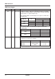
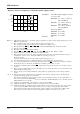
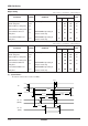
200
150
100
50
(µA)
I (1)
DD
0 1234567
V
DD
(V)
SED1560
SED1561
SED1562
Conditions: The built-in power supply is on and
T1 = T2 = Low.
SED1560 V
5 – VDD = –12.5 V; 3
times amplified
SED1561 V
5 – VDD = –8.0 V; 3
times amplified
SED1562 V
5 – VDD = –6.0 V; 2
times amplified
Internal oscillation:
SED1560 R
f = 1 MΩ
SED1561 R
f = 1 MΩ
SED1562 R
f = 1 MΩ
Remarks: *16
- Dynamic current consumption (I), if the built-in power supply is used.
Notes: *1. Although the wide range of operating voltage is guaranteed, a spike voltage change during access to the
MPU is not guaranteed.
*2. The operating voltage range of the V
SS and V5 systems (see Figure 11).
The operating voltage range is applied if an external power supply is used.
*3. Pins A0, D0 to D7, RD (E), WR (R/W), CS1, CS2, FR, SYNC, M/S, C86, SI, P/S, T1 and T2.
*4. Pins CL, SCL, and RES
*5. Pins D0 to D7, FR, SYNC, CL0, and DY0
*6. Pins A0, RD (E), WR (R/W), CS1, CS2, CL, M/S, RES, C86, SI, SCL, P/S, T1, and T2.
*7. Applied if pins D0 to D7, FR, and SYNC are high impedance.
*8. The resistance when the 0.1-volt voltage is applied between the “On” output terminal and each power
terminal (V1, V2, V3 or V4). It must be within the operating voltage (2).
R ON = 0.1 V/∆I
(∆I is the current that flows when 0.1 VDC is applied during power-on.)
*9. The relationship between the oscillation frequency, frame and Rf value (see Figure 10).
*10. “tr” (reset time) indicates the period between the time when the RES signal rises and when the internal
circuit has been reset. Therefore, the SED156
*
is usually operable after “tr” time.
*11. Specifies the minimum pulse width of RES” signal. The Low pulse greater than “
tRW” must be entered
for reset.
*12. If the voltage is amplified three times by the built-in power circuit, the primary power V
SS must be used
within the input voltage range.
*13. The V
5 voltage can be adjusted within the voltage follower operating range by the voltage regulator
circuit.
*14, 15, 16 Indicates the current consumed by the separate IC. The current consumption due to the LCD panel
capacity and wiring capacity is not included.
The current consumption is shown if the checker is used, the display is turned on, the output status of
Case 6 is selected, and the SED1560D
0B is set to 1/64 duty, the SED1561D0B is set to 1/32 duty, and the
SED1562D
0B is set to 1/16 duty.
*14. Applied if an external clock is used and if not accessed by the MPU.
*15. Applied if the built-in oscillation circuit is used and if not accessed by the MPU.
*16. Applied if the built-in oscillation circuit and the built-in power circuit are used (T1 = T2 = Low) and if
not accessed by the MPU. Measuring conditions: C1 = 4.7 µF, C2 = 0.47 µF, Ra + Rb = 2 MΩ
This includes the current that flows through the voltage regulator resistor (Ra + Rb = 2 MΩ). If the
built-in power circuit is used, the current consumption is equal to the current of V
SS power.