
Specifications
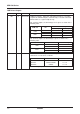
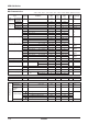
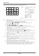
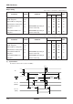

SED1560 Series
EPSON
7–17
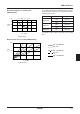
VSS = –5.0 ±10%, Ta = –30 ~ 85 °C
Item Signal Symbol Conditions Min. Max. Unit
Address hold time A0, CS
tAH8 10 ns
Address setup time
tAW8 10 ns
System cycle time
tCYC8 200 ns
Control L pulse width (WR) WR
tCCLW 22 ns
Control L pulse width (RD) RD
tCCLR 77 ns
Control H pulse width (WR) WR
tCCHW 172 ns
Control H pulse width (RD) RD
tCCHR 117 ns
Data setup time
tDS8 20 ns
Data hold time
tDH8 10 ns
RD access time D0 to D7
tACC8 CL = 100pF 70 ns
Output disable time
tCH8 10 50 ns
Input signal change time
tr, tf 15 ns
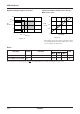
VSS = –2.7 ~ –4.5 V, Ta = –30 ~ 85 °C
Item Signal Symbol Conditions Min. Max. Unit
Address hold time A0, CS
tAH8 0ns
Address setup time
tAW8 0ns
System cycle time
tCYC8 450 ns
Control L pulse width (WR) WR
tCCLW 44 ns
Control L pulse width (RD) RD
tCCLR 194 ns
Control H pulse width (WR) WR
tCCHW 394 ns
Control H pulse width (RD) RD
tCCHR 244 ns
Data setup time
tDS8 20 ns
Data hold time
tDH8 10 ns
RD access time D0 to D7
tACC8 CL = 100pF 140 ns
Output disable time
tCH8 10 100 ns
Input signal change time
tr, tf 15 ns
Notes: 1. When using the system cycle time in the high-speed mode, it is limited by
tr + tf ≤ (tCYC8–tCCLW–
tCCHW) or tr + tf ≤ (tCYC8–tCCLR–tCCHR)
2. All signal timings are limited based on the 20% and 80% of V
SS voltage.
3. Read/write operation is performed while CS (CS1 and CS2) is active and the RD or WR signal is in the
low level.
If read/write operation is performed by the RD or WR signal while CS is active, it is determined by the
RD or WR signal timing.
If read/write operation is performed by CS while the RD or WR signal is in the low level, it is deter-
mined by the CS active timing.
4. When usingin the range of V
SS = –2.4 ~ –4.5V, raise the above ratings for –2.7 ~ –4.5V equally by 30%.