
User`s manual


DemoKit-LG2 User’s Manual
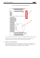
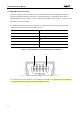
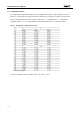
3.7 SB1, SB3, SB4, SB5 and SB6 Soldering Bridges
The SB1, SB3, SB4, SB5 and SB6 soldering bridges allow the board to be configured in a variety of
ways, as described in Table 2.
Figure 5. Soldering Bridges
1 2 3
1 2 3
SB1
SB5
SB6
3 2 1
3 2 1
SB3
SB4
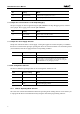
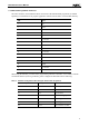
Table 2. Soldering Bridge Settings
Soldering Bridge Pad Setting Configuration
Closed (default) VCC connected to AVREF pin
SB1 1–2
Open V
CC disconnected from AVREF pin
1–2
2–3
Closed (default)
Open (default)
Subclock oscillator connected to P123/XT1 pin
SB3
1–2
2–3
Open
Closed
P123/XT1 pin connected to CN5–2
1–2
2–3
Closed (default)
Open (default)
Subclock oscillator connected to P124/XT2 pin
SB4
1–2
2–3
Open
Closed
P124/XT2 pin connected to CN5–4
1–2
2–3
Closed (default)
Open (default)
Main clock oscillator connected to P121/X1 pin
SB5
1–2
2–3
Open
Closed
P121/X1 pin connected to CN3–38
1–2
2–3
Closed (default)
Open (default)
Main clock oscillator connected to P121/X2 pin
SB6
1–2
2–3
Open
Closed
P121/X2 pin connected to CN3–40
Cutting the default connections (pad 1–2) of soldering bridges SB3/SB4 and SB5/SB6, respectively,
and closing pads 2–3 connects the corresponding MCU signals to the CN3 and CN5 external
connectors, respectively. In this mode, the MCU pins can be used as standard I/O ports, but you must
configure the MCU’s clock generator accordingly.
Note: Do not close the connection for the clock oscillator and external connectors at the same time. This
can have a negative effect on the operation of the subclock and main clock oscillators.
9