Maintenance Manual Prism HP / LPE-200 SCAN And SYSTEM PORTABLE RADIOS 800 MHz tab ericssonz
AE/LZB 119 1641 R1B MANUAL REVISION HISTORY REVISION R1A R1B DATE OCT 1995 JUL 1996 REASON FOR CHANGE Original issue Add LPE-200 info. Correct Assembly Diagrams and Parts List NOTICE! This manual covers Ericsson and General Electric products manufactured and sold by Ericsson Inc. NOTICE! Repairs to this equipment should be made only by an authorized service technician or facility designated by the supplier.
AE/LZB 119 1641 R1B TABLE OF CONTENTS SPECIFICATIONS......................................................................................................................................................................4 GENERAL...............................................................................................................................................................................4 DIGITAL ...................................................................................................
AE/LZB 119 1641 R1B TABLE OF CONTENTS (Con’t) INTRODUCTION ERROR CODES .....................................................................................................................................22 Error Code Overview.........................................................................................................................................................22 Error Code Format ...............................................................................................................
AE/LZB 119 1641 R1B SPECIFICATIONS∗ (Con't) DIGITAL AEGIS: Vocoding Method Data Rate Error Corr. Eff: Cryptographic (Optional): Encryption Tech: Key Permutations: Key Storage: Adaptive Multiband Encoding 9600 BPS 8.3 dB at 5% BER Non Linear/Block Transformation 1.8 x 10¹⁹ VGE Algorithm 7.2 x 10¹⁶ DES Algorithm 8 banks of 7 keys RECEIVE Channel Spacing 25/12.5 kHz (NPSPAC) Sensitivity (12 dB SINAD) 0.28 µV Spurious and Image Rejection -70 dB Selectivity: @ 12.
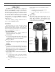
AE/LZB 119 1641 R1B DESCRIPTION The Ericsson Inc. Prism HP and LPE-200 Portable Radios are rugged, high-quality, high-performance FM twoway communications unit designed to operate in either ANALOG or DIGITAL environments. It is available in either Scan or System versions. These are Ericsson’s smallest and most sophisticated high-specification portable radios, designed to meet worldwide requirements.
AE/LZB 119 1641 R1B MECHANICAL The radios are packaged in a polycarbonate blend exterior housing. A six-cell back mounted nickel cadmium battery pack provides a nominal 7.5 volts. Two different nickel cadmium battery packs offering high and extended capacities are available for use with the portable radios. The top of the radio has a Volume, Channel/ Area/System select knob, Emergency/Home button, TX LED and a screw-on antenna mount connector.
AE/LZB 119 1641 R1B OPERATION The Prism series of portable radios is designed for EDACS and conventional mode operation. When the unit is used in a trunked EDACS, the digital control channel is automatically monitored. When the user initiates a call, the unit sends a digital request through a control channel to the site controller. The site controller then assigns the calling radio and all members of the talk group to an available working channel.
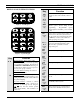
AE/LZB 119 1641 R1B KEYPAD SCAN/SYSTEM FUNCTIONS Key Function (Scan only) Adds/Deletes selected groups or channels from the Scan list of the currently selected system. SCN Turns the Scan operation On and Off. A/D (Scan only) Figure 2 - Scan Keypad OPT (Scan only) 1 (System only) 1-9, *, 0, # 2 3 * # 4 6 9 (System only) Figure 3 - System Keypad Key ▲ ▼ Function Primary Function: Allows user to select either system, groups, or channels, depending on personality programming.
AE/LZB 119 1641 R1B storage and personality storage. This software supports read/write of EEPROM data such as Tracking Data and Feature Encryption. Data compression is used to reduce FLASH application loading time. CIRCUIT ANALYSIS The portable radio is unique in the generation of the transmit carrier. The transmit section has an offset frequency loop operating at 134.4 MHz. This means the synthesizer is operating at a frequency that is not harmonically related to the output frequency.
AE/LZB 119 1641 R1B Local Oscillator Buffer (V450) The injection frequency (940.4-958.4 MHz) from the synthesizer circuit is applied to the base of Local Oscillator (LO) NPN buffer transistor V450 through capacitor C450 and inductor L450. This signal at the input of V450 is 0 dBM and is amplified to +4 dBm. This signal can be metered at TP450. The output of V450 is connected to the input of mixer Z402 (Pin 1).
AE/LZB 119 1641 R1B for 12.5 kHz channel mode. The selection of operation is controlled by HILLARY (D701). Selecting a preprogrammed digital or conventional channel causes an input from D701 to be applied on the base of inverter transistor V551. This places an input on bilateral switch N553 (Pins 12 & 13). If this input is +5 Volts, the 450 NARROW filter is switched into the circuit and the 450 WIDE filter is switched out of the circuit.
AE/LZB 119 1641 R1B TRANSMITTER Transmit Frequency Generation The main VCO, in the synthesizer circuit, is programmed to generate the 1st LO receive injection frequency (940.4 to 959.4 MHz). This carrier frequency is mixed with a transmit offset frequency of 134.4 MHz to generate the carrier and two side band frequencies. The carrier and upper side band are suppressed and only the lower side band is transmitted. For example: the carrier frequency of 940.4 MHz minus the offset frequency of 134.
AE/LZB 119 1641 R1B (MODQ and MODQ_B). The I input passes through a low pass filter consisting of capacitors C191, C192 and C193, resistor R166 and inductors L156 and L157. The output of this filter connects to N150, Pins 43 (I) and 42 (I_bar). The Q input passes through a low pass filter consisting of capacitors C194, C195 and C196, resistor R167 and inductor L158 and L159. The output of this low pass filter connects to N150, Pins 41 (Q) and 40 (Q_bar).
AE/LZB 119 1641 R1B anode, a reference voltage of 0.15 volts is on N102-A, Pin 3 (+IN). Forward biasing V103-2 causes a current to flow through directional coupler W100, Pins 6 and 9 (PORT 3 and PORT 4). This circuit provides temperature compensation for power detection. A voltage directly proportional to the RF power output is applied to N102-A, Pin 2 (-IN). This is due to the rectification of the coupled RF energy into V103-2.
AE/LZB 119 1641 R1B the proper device. The main synthesizer can be programmed in 12.5 kHz steps. These inputs can be metered at TP205 (CLOCK), TP206 (DATA) and TP207 (STROBE 1). Bilateral Switch (N201) Bilateral Switch N201 selects the loop filter required for programming the main VCO in 12.5 kHz steps. A +5 Volt signal (LOOP_SEL) from HILLARY connects to N201, Pin 5 (2_C Control) causing N201 to switch in the required resistor-capacitor combinations.
AE/LZB 119 1641 R1B resistor for RX_ON. Regulator N490 is normally enabled. When RX_ON goes high, V490 conducts and N490 is enabled. The control voltage can be metered at test point TP490. With N490 enabled a regulated 5.5 Volts is on N490, Pin 4 (Vout). This voltage can be metered at TP491. Capacitor C491 provides line filtering.
AE/LZB 119 1641 R1B Low Battery Power Down The battery voltage is monitored with A/D input to ATTIE. To protect the battery against deep discharge conditions a LOW_BATT_PWR_OFF line is provided to shut the radio down until a fresh battery is attached. When the battery voltage falls below 5.6 Volts, diode V900 is forward biased conducting through V902. When the LOW_BATT_PWR_OFF line is switched high, V901 and V902 latch on forcing enable pin N900-3 high, which results in shutting the radio off.
AE/LZB 119 1641 R1B Flash Programming 3. Power the radio ON. Release the buttons. The “FLASH” software is the current version of the Prism HP radio operating software. When changes and enhancements are made to the operating code, the new operating code can be “FLASHED” to the radio, upgrading the operating code without any hardware changes to the radio. Flash software is simply a computer file which is read from a disk and downloaded to the radio using the EDACS3 PC Programmer.
AE/LZB 119 1641 R1B Table 1 - General Troubleshooting Symptom Possible Cause/Action Required Completely Inoperative (no display or audio on power up) Power Supply Problem? 1. Check battery voltage with a voltmeter. 2. Charge battery or replace battery. 3. Check to be sure battery contacts are not broke or bent. 4. Clean battery contacts. 5. Check Fuse (F190). At power -up an error message is displayed. 1.
AE/LZB 119 1641 R1B NOTE Receive RF levels measured with a -50 dBm signal injected at the antenna port. NOTE Transmit levels measured using a mid-band frequency and high power.
AE/LZB 119 1641 R1B ERROR CODES INTRODUCTION This section lists all the radio errors and warnings. The radio displays errors and warnings to the user to indicate problems that have occurred. Radio errors can occur at any time from power up to power down. Each error code in the list includes an explanation of what went wrong and what action to take to correct the problem. Error codes are divided into three categories: • Fatal operational error codes. These errors will cause the radio to reset.
AE/LZB 119 1641 R1B Non-Fatal Errors Non-fatal errors are displayed for a short period (about two seconds) then normal radio operation will resume. Non-Fatal Errors Description Undocumented error. Feature encryption error. DSP error. Attempt to keyload w/o bank storage. Attempt to keyload w/o private DSP file loaded.
AE/LZB 119 1641 R1B FATAL_LCD_NOACK FATAL_LCD_HARD_FAIL FATAL_SCI_NOHEAP HARDWARE HARDWARE HARDWARE 40 41 50 FATAL_DSP_NOACK FATAL_DSP_FIFOOVR FATAL_DSP_BADMSG FATAL_DSP_WRONGRESP FATAL_DSP_TWOACKS FATAL_DSP_NORESOURCE FATAL_BL_NOHEAP FATAL_BL_SCI_ATTACH FATAL_RXSIF HARDWARE HARDWARE HARDWARE HARDWARE HARDWARE HARDWARE HARDWARE HARDWARE HARDWARE 60 61 62 63 64 65 91 92 98 LCD did not ack message. LCD hardware is invalid. Serial communication interface out of heap (RAM memory) space.
AE/LZB 119 1641 R1B PI_MALLOC_ERROR SOFTWARE 503 UI_FATAL_DEVICE_ERROR UI_FATAL_SWTO_MALLOC_ERROR UI_FATAL_SWTO_MAX_ERROR UI_FATAL_WINDOW_MAX_ERROR UI_FATAL_WINDOW_MALLOC_ERROR UI_FATAL_MESSAGE_INVPARM PERSDATA SOFTWARE SOFTWARE SOFTWARE SOFTWARE SOFTWARE 600 601 602 603 604 605 UI_FATAL_RI_MSGBUF_FULL SOFTWARE 606 UI_FATAL_RISYS_MSGBUF_FULL SOFTWARE 607 UI_FATAL_CI_MSGBUF_FULL UI_FATAL_DEVICE_NOTSUPPORTED SOFTWARE PERSDATA 608 609 UI_FATAL_AUXIO_MALLOC_ERROR UI_FATAL_NET_DEVICE_ERROR UI_FATA
AE/LZB 119 1641 R1B Error Name PIFEAT_SNR_ERROR Message FEAT ERR Code 550 PIFEAT_READ_ERROR FEAT ERR 551 PIFEAT_CRC_ERROR FEAT ERR 552 RI_DSPDOWN_NOATTEMPT RI_DSPDOWN_NOTFOUND RI_DSPDOWN_CRCFAIL RI_DSPDOWN_ENCERR RI_DSPDOWN_PMFAIL DSP ERR DSP ERR DSP ERR DSP ERR DSP ERR 850 851 852 853 854 RI_DSPDOWN_DMFAIL DSP ERR 855 RI_DSPDOWN_BIOSERR AEGIS_KEYLOAD_NOBANKS AEGIS_PVT_NONE DSP ERR NO KBANK NO PVT 856 860 870 Description Feature encryption - Cannot read radio ROM serial number.
AE/LZB 119 1641 R1B Radio- Canceled by receiver Radio- Canceled by sender Radio- End of transmission received Radio- Transmit error 15 16 17 18 Radio- Invalid command Radio- No application code 19 20 Radio- Application code error Radio- EEPROM programming error Radio- Baud rate has changed 21 22 23 The radio operating software received a cancel command. The radio software received or sent an end of transmission. Radio could not transmit the required data.
AE/LZB 119 1641 R1B DISASSEMBLY PROCEDURE Figure 11 5. To disassemble the Prism radio: Figure 9 1. Remove the battery pack by pushing the battery release button and sliding the battery pack straight back until it stops, then lift the battery pack out. When replacing the battery pack align the ribs on the sides of the battery pack with the slots in the sides of the radio. Push down and slide the battery pack into place.
AE/LZB 119 1641 R1B Figure 13 Figure 15 10. Using a flat blade screwdriver, push on the battery contacts. Be careful not to damage the gasket. Applying pressure on the battery contacts will slowly separate the main circuit board and shield from the metal frame. 12. Remove the board from the shield by prying up on a corner and working around the board to release the snaps. Figure 13 - Push Battery Contacts Figure 14 11. Carefully unplug the small flex at the top of the radio (F).
AE/LZB 119 1641 R1B Figure 17 14. Pry up on the hook to release from the latch and push down on the switches to remove the assembly from the housing. PA Module Replacement Remove the PA Module by unsoldering the five (5) leads attached to the Main Board (see the Outline Diagram). Solder new module in same location. Filters Z400 And Z401 Replacement Filter Z400 has four (4) leads that go all the way through the board and are soldered on the reverse side of the board. Unsolder the four leads to remove Z400.
ASSEMBLY DIAGRAM AND PARTS LIST AE/LZB 119 1641 R1B Prism Radio 800 MHz SYMBOL PART NUMBER DESCRIPTION 1 SXK 107 3807 Front Assembly (Scan) 1 SXK 107 3807/2 Front Assembly (LPE-200 Scan) 1 SXK 107 3808 Front Assembly (System) 1 SXK 107 3808/2 Front Assembly (LPE-200 System) 2 SXK 107 3814 Rear Assembly (807.5 - 824 MHz TX) 2 SXK 107 3814/2 Rear Assembly (806 - 824 MHz TX) MARRIAGE HARDWARE KIT 3 SXA 120 4145 Main Gasket 4 SXA 124 025/0080 Screw (2) 6 SXA 120 4118 Washer Stop.
AE/LZB 119 1641 R1B ASSEMBLY DIAGRAM AND PARTS LIST Front Assembly (Scan) SXK 107 3807 SYMBOL PART NUMBER DESCRIPTION Front Cover 1 2 SXA 120 4112 Keypad Scan 2 SXA 120 4112/02 Keypad Scan (LPE-200) 3 SXA 120 4122 Keypad Retainer 4 ROA 117 2216 Flex Assembly/Printed Bd 6 SXA 120 4119 Speaker Gasket 7 RLE 906 18/2 Loudspeaker 8 SXA 120 4121 PTT Actuator 9 SXA 120 4120 Side Control Bezel 10 SXA 120 4136 Side Control Keypad 11 SXA 120 4128 Gasket: UDC PWB 12 SXA 120 4129 Ga
ASSEMBLY DIAGRAM AND PARTS LIST AE/LZB 119 1641 R1B Front Assembly (System) SXK 107 3808 SYMBOL PART NUMBER DESCRIPTION Front Housing 1 2 SXA 120 4115 Keypad (System) 2 SXA 120 4115/02 Keypad System (LPE-200) 3 SXA 120 4122 Keypad Retainer 4 ROA 117 2216 Flex Assembly/Printed Bd 6 SXA 120 4119 Speaker Gasket 7 RLE 906 18/2 Loudspeaker 8 SXA 120 4121 PTT Actuator 9 SXA 120 4120 Side Control Bezel 10 SXA 120 4136 Side Control Keypad 11 SXA 120 4128 Gasket: UDC PWB 12 SXA 120
AE/LZB 119 1641 R1B ASSEMBLY DIAGRAM AND PARTS LIST Rear Assembly SXK 107 3814 SYMBOL PART NUMBER DESCRIPTION 1 SXK 107 3816 Rear Housing Casting 2 SXA 120 4110 Rear Cosmetic Cover 3 RNT 403 351/01 Antenna Switch Assembly 3 SXA 120 4137 RF Gasket Nut 3 4 SXA 120 4133 Switch Retainer 5 ROA 117 2220 Switch Module Assembly 6 SXA 120 4134 Switch Gasket Assembly 7 ROA 117 2212 DSP Module 8 ROA 117 2201 Main Board Asm (807.
ASSEMBLY DIAGRAM AND PARTS LIST AE/LZB 119 1641 R1B 800 MHz Main Board Assembly ROA 117 2201 SYMBOL PART NUMBER 1 DESCRIPTION Printed Circuit Board N101 RYTUA 901 07/01 PA Module X101 RPT 403 303/01 Battery Connector Z400 RTN 202 699/01 Filter Z401 RTN 202 728/01 Filter * COMPONENTS ADDED, DELETED, OR CHANGED BY PRODUCTION CHANGES. 800 MHz Main Circuit Board Assembly (151 88-ROA 117 2201, Rev.
AE/LZB 119 1641 R1B ASSEMBLY DIAGRAM AND PARTS LIST RF/LOGIC SHIELD SXK 107 3818 SYMBOL PART NUMBER DESCRIPTION 1 SXA 120 4111 Shield 2 SXA 120 4139 Shield Wall 3 SXA 120 4149 Speaker Pad 4 SXA 120 4148 Shield Insulator * COMPONENTS ADDED, DELETED, OR CHANGED BY PRODUCTION CHANGES. RF/Logic Shield (151 88-SXK 107 3818, Rev.
AE/LZB 119 1641 R1B This page intentionally left blank 37
AE/LZB 119 1641 R1B OUTLINE DIAGRAM FRONT SIDE 800 MHz Circuit Board (1078-ROA 117 2201 Uen, Sheet 1, Rev.
OUTLINE DIAGRAM AE/LZB 119 1641 R1B BACK SIDE 800 MHz Circuit Board (1078-ROA 117 2201 Uen, Sheet 2, Rev.
AE/LZB 119 1641 R1B Block Diagram (1911-ROA 117 2201/1, Sheet 1, Rev.
SCHEMATIC DIAGRAM AE/LZB 119 1641 R1B Transmitter (1911-ROA 117 2201/1, Sheet 2, Rev.
AE/LZB 119 1641 R1B Transmit Offset (1911-ROA 117 2201/1, Sheet 3, Rev.
SCHEMATIC DIAGRAM AE/LZB 119 1641 R1B Synthesizer (1911-ROA 117 2201/1, Sheet 4, Rev.
AE/LZB 119 1641 R1B Receiver Front End (1911-ROA 117 2201/1, Sheet 5, Rev.
SCHEMATIC DIAGRAM AE/LZB 119 1641 R1B Receiver Back End (1911-ROA 117 2201/1, Sheet 6, Rev.
AE/LZB 119 1641 R1B RF Regulators (1911-ROA 117 2201/1, Sheet 7, Rev.
SCHEMATIC DIAGRAM AE/LZB 119 1641 R1B Digital I/O Lines to RF Section (1911-ROA 117 2201/1, Sheet 8, Rev.
AE/LZB 119 1641 R1B Analog I/O Lines to RF Section (1911-ROA 117 2201/1, Sheet 9, Rev.
SCHEMATIC DIAGRAM AE/LZB 119 1641 R1B TX/RX Audio (1911-ROA 117 2201/1, Sheet 10, Rev.
AE/LZB 119 1641 R1B TX/RX Audio (1911-ROA 117 2201/1, Sheet 11, Rev.
SCHEMATIC DIAGRAM AE/LZB 119 1641 R1B Flex Connector (1911-ROA 117 2201/1, Sheet 12, Rev.
AE/LZB 119 1641 R1B DSP Connectors (1911-ROA 117 2201/1, Sheet 13, Rev.
SCHEMATIC DIAGRAM AE/LZB 119 1641 R1B System Memory (1911-ROA 117 2201/1, Sheet 14, Rev.
AE/LZB 119 1641 R1B Regulators/Power Switch (1911-ROA 117 2201/1, Sheet 15, Rev.
SCHEMATIC DIAGRAM AE/LZB 119 1641 R1B LCD Bias, LED Driver, UDC SWA+ OUT (1911-ROA 117 2201/1, Sheet 16, Rev.
AE/LZB 119 1641 R1B Attie D601 (1911-ROA 117 2201/1, Sheet 17, Rev.
SCHEMATIC DIAGRAM AE/LZB 119 1641 R1B Hillary D701 (1911-ROA 117 2201/1, Sheet 18, Rev.
AE/LZB 119 1641 R1B This page intentionally left blank Ericsson Inc. Private Radio Systems Mountain View Road Lynchburg, Virginia 24502 1-800-528-7711 (Outside USA, 804-528-7711) AE/LZB 119 1641 R1B Printed in U.S.A.