
Specifications

AE/LZB 119 1641 R1B
14
(MODQ and MODQ_B). The I input passes through a low
pass filter consisting of capacitors C191, C192 and C193,
resistor R166 and inductors L156 and L157. The output of
this filter connects to N150, Pins 43 (I) and 42 (I_bar). The
Q input passes through a low pass filter consisting of
capacitors C194, C195 and C196, resistor R167 and
inductor L158 and L159. The output of this low pass filter
connects to N150, Pins 41 (Q) and 40 (Q_bar). The I and
Q inputs are summed with the lower side band then the
outputs of these mixer circuits are summed to produce the
lower side band with transmit modulation. This signal is
amplified and connected through N150, Pin 34 (DUAL TX)
to the input of a transmit band pass filter.
Transmit Band Pass Filter
The TX_RF signal (0 dBm) connects through coupling
capacitor C125 to the input of a TX Band Pass Filter.
Filtering of the TX_RF line is provided by capacitor C126.
The TX Band Pass Filter is tuned to the transmit carrier
frequency by applying control voltage RX_TX _TUNE.
RX_TX TUNE comes from ATTIE D601 (DAC02). This
control voltage ranges typically from 1 to 4 volts and can be
metered at test point TP100. This control voltage is applied
through resistors R101 and R102 to the cathodes of variable
capacitors V105 and V106 respectively. This application
varies the capacitance of V105 and V106, to tune the filter
to the lower side band of the transmit carrier frequency. The
actual carrier frequency and the upper sideband are
attenuated. The lower sideband output of the band pass
filter (-8 dB) connects through coupling capacitors C121 and
C139 to the base of buffer amplifier transistor V104.
Filtering is provided by capacitor C120.
Buffer Amplifier (V104)
When transmitting the collector voltage for transistor
V104 is provided through PIN diode V101 and is controlled
by DPTT. The collector voltage is typically 4.1Vdc. The
base voltage of V104 is typically 1.9 Volts and the emitter
voltage is typically 1.2 Volts. The emitter voltage can be
metered at test point TP101. The RF output from the
collector (+3 dBM) connects through coupling capacitor
C116 and resistor R105 to power amplifier N101, Pin 1
(Pin/Vc).
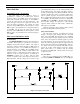
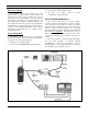
Power Amplifier (N101)
Power amplifier N101 is a three stage Class C operated
RF power amplifier module designed to operate over the
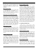
frequency range of 806-870 MHz (see Figure 5).
1
2 34 5
PoutVdd3Vdd2Vdd1Pin/Vc
Figure 5 - Power Amplifier
B+ (7.2 Vdc) connects to N101 through RF chokes
L114-1, L114-2 and L114-3. Additional RF filtering of the
B+ line is provided by capacitors C132 through C137. This
voltage is applied to N101, Pin 2 (Vdd1), Pin 3 (Vdd2) and
Pin 4 (Vdd3). Vdd1, 2 and 3 refers to drain voltages 1, 2
and 3 shown above. The RF input from the buffer amplifier
circuit and the power control voltage from Power Control
Buffer N102-A is applied to N101, Pin 1 (Pin/Vc). The + 3
dB on the input of N101 is amplified to 3 watts on the
output. This output can be regulated by the power control
circuit to as low as 0.1 watts by means of the DC level at Pin
1. The output on N101, Pin 5 (+) connects through inductor
L106 and filter capacitor C115 to Directional Coupler
W100, Pin 4 (PORT 2).
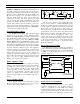
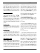
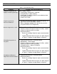
Directional Coupler (W100)
The RF output connected to W100, Pin 4 (PORT 2)
connects directly through W100 to Pin 1 (PORT 1) where it
is output to the antenna circuit. The connection between Pin
9 (PORT 3) and Pin 6 (PORT 4) is part of the sensing
circuit (See Figure 4).
2
4
5
6
7
9
10
RF Input
RF Output
Port 1 Port 2
Port 3 Port 4
GND GND
50 Ohms
Power Sense
Circuit N102-A
8
3
1
Figure 6 - Directional Coupler
Power Sensor Circuit (N102-A)
The power sensor circuit consist of part of W100,
comparator amplifier N102-A and associated circuitry in
between. A regulated 5.5 volts (VTX) from transmit
regulator N190 is applied to N102-A, Pin 8, (V+). This
voltage forward biases Schottky diodes V103-1 and V103-2.
When forward biased diode V103-1 has 0.3 volts on the