ES1869 AudioDrive® Solution Data Sheet DESCRIPTION The ES1869 AudioDrive® solution is a mixed-signal single chip that adds 16-bit stereo sound and FM music synthesis to personal computers. It is compliant with Microsoft® PC 97 and PC 98 specifications and WHQL audio requirements.
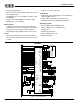
ES1869 DATA SHEET FEATURES • Integrated dual game port • I2S Zoom Video port interface with a sample rate up to 48 • Supports 3.3 V or 5.0 V operation Compatibility • Supports PC games and applications for Sound Blaster™ and Sound Blaster™ Pro kHz for MPEG audio • Serial port interface to external DSP (e.g.
ES1869 DATA SHEET CONTENTS CONTENTS DESCRIPTION . . . . . . . . . . . . . . . . . . . . . . . . . . . . . . . . . . . . 1 FEATURES . . . . . . . . . . . . . . . . . . . . . . . . . . . . . . . . . . . . . . . 1 PINOUT . . . . . . . . . . . . . . . . . . . . . . . . . . . . . . . . . . . . . . . . . 5 PIN DESCRIPTION . . . . . . . . . . . . . . . . . . . . . . . . . . . . . . . . 6 FUNCTIONAL DESCRIPTION . . . . . . . . . . . . . . . . . . . . . . . . 9 Digital Subsystems . . . . . . . . . . . . . . . . . .
ES1869 DATA SHEET TABLES Pop Prevention in the External Amplifier . . . . . . . . .77 Power Management and the FM Synthesizer . . . . .78 Self-Timed Power-Down . . . . . . . . . . . . . . . . . . . . . . . . .78 Enabling Self-Timed Power-Down . . . . . . . . . . . . . .78 General-Purpose Outputs and Power-Down . . . . . . . . .78 ELECTRICAL CHARACTERISTICS . . . . . . . . . . . . . . . . . . .79 Absolute Maximum Ratings . . . . . . . . . . . . . . . . . . . . . .79 Thermal Characteristics . . . . . . . . .
ES1869 DATA SHEET PINOUT VDDD XO XI GNDD IOWB IORB IRQA IRQB IRQC IRQD IRQE IRQF DACKBA DRQA DACKBB DRQB DACKBC DRQC DACKBD / IISCLK DRQD / IISDATA MODE MSI MSO VDDD GPO0 / GPCS MMCSB / IISLR MMIRQ / PCSPKI MMIEB / PCSPKO GNDD AOUT_R PINOUT 81 80 79 78 77 76 75 74 73 72 71 70 69 68 67 66 65 64 63 62 61 60 59 58 57 56 55 54 53 52 51 50 82 49 83 48 84 47 85 46 86 45 87 44 88 43 89 42 90 41 ES1869F 91 92 40 39 93 38 94 37 95 36 96 35 97 34 98 33 99 32 100 1 2 3 4 5
ES1869 DATA SHEET PIN DESCRIPTION PIN DESCRIPTION Name Number A[11:0] 99,100,1,2,6:4, 10:8,97,98 I Address inputs from the ISA bus. VDDD 3,57,80 I Digital supply voltage (5 V ± 10%). GNDD 7,24,52,77 I Digital ground. 11 I Active-low address enable from the ISA bus. AEN D[7:0] 19:12 I/O Description I/O ISA bidirectional data bus. I PSEL 20 SECS Selects the PnP ROM device used: 0 Internal ROM 1 93LC66 – 512 x 8, 9 address bits I/O Serial EEPROM CS. This is an input pin during RESET.
ES1869 DATA SHEET PIN DESCRIPTION Name Number I/O Description FOUT_L 45 O Filter output left. FOUT_L is AC-coupled externally to CIN_L to remove DC offsets. This output has an internal series resistor of about 5k ohms. A capacitor to analog ground on this pin can be used to create a low-pass filter pole that removes the switching noise introduced by the switched-capacitor filter. CIN_L 46 I Capacitive coupled input left. CIN_L has an internal pull-up resistor to CMR of approximately 50k ohms.
ES1869 DATA SHEET PIN DESCRIPTION Name Number I/O Description XO 79 O Crystal oscillator output. Connect to external 14.318 MHz crystal. RESET 81 I Active-high reset from the ISA bus. FSR 82 I Input with internal pull-down. Frame sync for receive data from external DSP. Programmable for active-high or active-low. FSX 83 I Input with internal pull-down. Frame sync for transmit request from external DSP. Programmable for active-high or active-low.
ES1869 DATA SHEET FUNCTIONAL DESCRIPTION FUNCTIONAL DESCRIPTION This section shows the overall structure of the ES1869 and discusses its major functional subunits. GNDD VDDD The major subunits of the ES1869 are shown in Figure 4 and described briefly in the following paragraphs. CIN FOUT CMR GPI GPO PCSPKI AUXB MIC VOL. CTRL.
ES1869 DATA SHEET FUNCTIONAL DESCRIPTION Digital Subsystems Analog Subsystems • RISC microcontroller – game-compatible audio • Record and Playback Mixers – seven input stereo functions are performed by an embedded microcontroller. • Oscillator – circuitry to support an external crystal. • ROM and RAM – firmware ROM and data RAM to the embedded microcontroller.
ES1869 DATA SHEET MIXER SCHEMATIC BLOCK DIAGRAM MIXER SCHEMATIC BLOCK DIAGRAM ADC/DAC Output Volume DMA 1 digital audio DAC DMA 2 digital audio Preamp MIC LINE HWWT FM X Playback Mixer DAC I2S Mono_In AUXA Record Monitor Off AUXB On Master Volume AOUT Record Source Record Mixer ADC Input Volume Figure 5 ES1869 Mixer Schematic Block Diagram ESS Technology, Inc.
ES1869 DATA SHEET BUS INTERFACING BUS INTERFACING This section discusses interfacing to the PC bus, and items relating to configuration for the bus. Table 1 shows the pins used to interface the ES1869 to the ISA bus. Table 1 ISA Bus Interface Pins Pins Descriptions A[15:12] Dual-purpose pins. A[15:12] are ISA bus address inputs. A[11:0] ISA bus address inputs. AEN ISA active-low address enable. D[7:0] ISA bidirectional data bus. DRQD Dual-purpose pin. DRQD is a tri-state output.
ES1869 DATA SHEET DIGITAL AUDIO DIGITAL AUDIO The ES1869 incorporates two digital audio channels. There are three sources of DMA requests and three targets for DMA acknowledge: to enable the different transfers vary depending on which DMA channel and which mode (Compatibility or Extended) is used. Audio 1 The first audio channel. This channel is used for Sound Blaster Pro compatible DMA, Extended mode DMA, and programmed I/O. It can be used for either record or playback.
ES1869 DATA SHEET DIGITAL AUDIO Before a DMA transfer, the application first programs the DMA controller for the desired transfer size and address, then programs the ES1869 with the same size information. At the end of the transfer, the ES1869 generates an interrupt request, indicating that the current block transfer is complete. The FIFO gives the application program sufficient time to respond to the interrupt and initiate the next block transfer.
ES1869 DATA SHEET DIGITAL AUDIO DMA mode is used when programming the second audio channel for transfers: • DMA modes – Normal (Single or Demand transfer) – Auto-Initialize (Single or Demand transfer) DRQ Latch Feature DRQ latching is enabled when bit 7 of PnP VendorDefined Card-Level register 25h is high.
ES1869 DATA SHEET DIGITAL AUDIO Pop sounds may still occur if the DAC level was left at a value other than mid-level (code 80h on an 8-bit scale) by the previous play operation. To prevent this, always finish a DAC transfer with a command to set the DAC level to mid-range: 10h + 80h 16 SAM0023-122898 ESS Technology, Inc.
ES1869 DATA SHEET INTERRUPTS INTERRUPTS There are seven interrupt sources in the ES1869, shown in Table 4. Table 4 ES1869 Interrupt Sources Interrupt Source Description Audio 1 An interrupt used for the first DMA channel (Sound Blaster compatible DMA, Extended mode DMA, and Extended mode programmed I/O), as well as Sound Blaster-compatible MIDI receive. Controller register B1h controls use of this interrupt for Extended mode DMA and programmed I/O.
ES1869 DATA SHEET INTERRUPTS Interrupt Mask Register Sharing Interrupts Port Config_Base+7h can be used to mask any of the seven interrupt sources. Plug and Play does not allow sharing of interrupts in its resource assignment decision making. If a device wants to share an interrupt with another device that has been assigned an interrupt by PnP, the first device cannot request an interrupt for itself.
ES1869 DATA SHEET PERIPHERAL INTERFACING PERIPHERAL INTERFACING I2S Serial Interface DSP Interface Three input pins, IISDATA, IISCLK, and IISLR, are used for a serial interface between an external device and a stereo DAC within the ES1869. These inputs can be left floating or connected to ground if the serial interface is not used. The ES1869 contains a synchronous serial interface for connection to a DSP serial interface. The typical application for this interface is a speakerphone.
ES1869 DATA SHEET PERIPHERAL INTERFACING 16-bit Stereo DAC 16-bit Stereo DAC DAC DAC DMA2 FIFO 16-bit Stereo CODEC ISA Bus DAC ADC DMA1 FIFO Mixer 16-bit Stereo CODEC ISA Bus Microphone FDXO DAC ADC Serializer/ Deserializer DAC DAC DMA2 FIFO Speaker DSP/CODEC Port Figure 9 Telegaming Mode DAC ADC DMA1 FIFO Microphone FDXO DAC ADC Serializer/ Deserializer Mixer Speaker DSP/CODEC Port Figure 10 Default Mode Telegaming Mode No Acoustic Echo Cancellation This mode is enabled when t
ES1869 DATA SHEET PERIPHERAL INTERFACING respectively. In addition, set bit 1 of Mixer register 46h high to enable FDXO as an output when DSP serial mode is enabled. The volume of the DSP digital audio playback is controlled within the DSP by scaling the data. Serial Data Format Figure 11 shows the format for serial data used with the DSP serial interface.
ES1869 DATA SHEET PERIPHERAL INTERFACING Modem Interface IDE CD-ROM Interface The ES1869 allows a direct interface to an external modem. There are four pins dedicated for an external modem. Table 9 identifies pins in the Modem interface. The ES1869 allows a direct interface to an IDE CD-ROM drive. There are four pins dedicated for an IDE CD-ROM interface. Table 10 identifies these pins.
ES1869 DATA SHEET PERIPHERAL INTERFACING General-Purpose I/O Device In addition to modem and CD-ROM interfaces, the ES1869 Plug and Play logic supports one generalpurpose I/O device. The GPO0 output can be configured to provide an active-high chip-select output when this device is accessed. The General-Purpose device can decode 1, 2, 4, 8, or 16 consecutive addresses.
ES1869 DATA SHEET PERIPHERAL INTERFACING JOYSTICK PORT 8 15 7 14 6 13 5 12 4 11 3 10 2 9 1 R3 220 R4 2.2K R1 10K R2 270 Q2 2N3904 Q1 2N3904 R5 5.6K C1 220pF 5 3 C2 220pF 2 4 1 DIN J1 MIDI OUT R6 270 D1 DB15P MIDI IN ISO1 5 2 4 1 3 DIN J2 Figure 15 MIDI Serial Interface EEPROM ROM Format Serial EEPROM Interface The ES1869 gets Plug and Play configuration data from an internal masked ROM or an external EEPROM device. The external EEPROM device is 512K x 8-bit in size.
ES1869 DATA SHEET PERIPHERAL INTERFACING MONO_IN and MONO_OUT MONO_IN is a line-level analog input. MONO_IN is an input to the playback mixer and the record mixer. The mixer volumes are controlled by mixer registers 6Dh (playback) and 6Fh (record). Alternately, MONO_IN can be mixed with AOUT_L and AOUT_R after the master volume stage. Bit 0 of mixer register 7Dh, when high, enables MONO_IN to be mixed directly (unity gain) with AOUT_L and AOUT_R.
ES1869 DATA SHEET PERIPHERAL INTERFACING For support of mixer master volume control, a write to mixer registers 22h or 32h translates automatically into writes to the master volume registers. Since register 22h only has 3-bit resolution per channel, and register 32h only has 4-bit resolution per channel, a translation circuit is included in the ES1869 that translates 3- or 4-bit volume values into the 6-bit volume + mute that is used in the master volume registers.
ES1869 DATA SHEET ANALOG DESIGN CONSIDERATIONS ANALOG DESIGN CONSIDERATIONS This section describes design considerations related to inputs and outputs of analog signals and related pins on the chip. Game Port The game port address 201h is decoded for timer pins TA, TB, TC, and TD, and switch pins SWA, SWB, SWC, and SWD. The MIDI serial input and output also come from the game port connector in most applications.
ES1869 DATA SHEET PNP CONFIGURATION AND REGISTERS PNP CONFIGURATION AND REGISTERS Card-Control Card-Level Registers Figure 20 shows the configuration register set that is discussed in the following pages. As shown below, the Card-Level registers supported by the ES1869 are the Card-Control Card-Level registers at addresses 00h-07h, and the Vendor-Defined Card-Level registers at addresses 20h-2Fh.
ES1869 DATA SHEET PNP CONFIGURATION AND REGISTERS Wake[CSN] 64, a3, c0, f3, e8, e5, 73, a8 c5, 61, 31, 19, f, 94, d9, 6f a6, 52, 2a, 14, 99, 4f, b4, cb f6, 7a, 3c, 8f, d4, f9, 7d, 3f , (03h, W) Data 7 6 5 4 3 2 1 0 If data written is 00h and it: Register 25h, bits 6:5 = 1,1 65, a2, c1, f2, e9, e4, 72, a9 c4, 60, 30, 18, e, 95, d8, 6e a7, 53, 2b, 15, 98, 4e, b5, ca f7, 7b, 3d, 8e, d5, f8, 7c, 3e , • matches the
ES1869 DATA SHEET PNP CONFIGURATION AND REGISTERS Resource Data (04h, R) IRQF, IRQE IRQF Resource data 7 6 5 4 3 (22h, R) 2 1 7 0 Returns next byte of resource data, provided the status bit in register 05h has been polled before each byte read, indicating that data is ready. Only works in Configuration mode. 6 IRQE 5 4 3 2 1 Defines IRQ number assigned to F and E pins. Loaded from Configuration ROM Header after PnP reset. Unused IRQ pins should be assigned IRQ #1.
ES1869 DATA SHEET PNP CONFIGURATION AND REGISTERS Bits Name Bit Definitions: Description Bits Name 1 CD-ROM 1 = CD-ROM is LDN 3 or 4. 0 = CD-ROM is not present. 0 MPU-401 1 = MPU-401 is LDN 3; interrupt is not shared with audio interrupt 1 or 2. 0 = MPU-401 is part of LDN 1; interrupt is shared with audio interrupt 1 or 2.
ES1869 DATA SHEET PNP CONFIGURATION AND REGISTERS Table 11 Logical Device Summary (Continued) LDN # After reset or after a 1 is written to the reset bit in the card’s configuration control bit, the default for this register is 0. Device Bit Definitions: 31h I/O Range Check. 60h I/O base address, bits 11:8. If zero, this device is disabled. Two locations. 61h I/O base address, bits 7:0. 70h Interrupt Request MPU Select. 71h Interrupt Request Type Select 0 (returns 2).
ES1869 DATA SHEET PNP CONFIGURATION AND REGISTERS FM Alias I/O Base Address Bit Definitions: Bits Name Description 0 0 0 0 2:0 Data Select which channel is in use for DMA 1. 7 6 5 4 LDN 1: Audio Device This device actually supports three functions: audio, FM, and MPU-401. Audio requires sixteen I/O locations, one interrupt which is shared with MPU-401, and two DMA channels. FM requires four I/O locations. MPU-401 requires two I/O locations.
ES1869 DATA SHEET PNP CONFIGURATION AND REGISTERS Interrupt Request Type Select 2 (73h, R) 0 0 0 0 0 0 1 0 7 6 5 4 3 2 1 0 Interrupt request type select 2. Returns 2 (low-to-high transition). DMA Channel 1 Select Bit Definitions: Bits Name Description 1 Enable range check 1 = Enable range check. 0 = Disable. 0 Pattern select 1 = 55h. 0 = AAh.
ES1869 DATA SHEET PNP CONFIGURATION AND REGISTERS I/O Decoder 0 Base Address 0 0 0 0 7 6 5 4 (60h, R/W) Bits Name A[11:8] 3 2 Bit Definitions: 1 0 1 Enable range check 1 = Enable range check. 0 = Disable. 0 Pattern select 1 = 55h. 0 = AAh. I/O base address, bits 11:8. Two locations. I/O Decoder 0 Base Address Description (61h, R/W) A[7:0] 7 6 5 4 3 2 1 0 I/O base address, bits 7:0.
ES1869 DATA SHEET PNP CONFIGURATION AND REGISTERS 7 6 5 4 3 2 1 0 Interrupt Request Modem Select Returns 4 (no DMA channel selected). Bit Definitions: Description 2:0 Data Select which DMA channel is in use for CD-ROM DRQ. LDN 5: Modem Device The Modem Device is optional. If present, it is LDN 3, 4, or 5. Activate 0 0 0 0 0 0 Activate 7 6 5 4 3 2 1 0 After reset or after a 1 is written to the reset bit in the card’s configuration control bit, the default for this register is 0.
ES1869 DATA SHEET PNP CONFIGURATION AND REGISTERS Bit Definitions: Bits Name Description 1 Enable range check 1 = Enable range check. 0 = Disable. 0 Pattern select 1 = 55h. 0 = AAh. I/O Decoder 0 Base Address 0 0 0 0 7 6 5 4 (60h, R/W) A[11:8] 3 2 1 0 I/O base address of address range, bits 11:8. Four, eight, or sixteen locations. I/O Decoder 0 Base Address (61h, R/W) A[7:0] 7 6 5 4 3 2 1 0 I/O base address of address range, bits 7:0.
ES1869 DATA SHEET I/O PORTS I/O PORTS Port Summary Table 12 I/O Ports for Configuration, Audio, FM, MPU-401, and Joystick Devices Port Read/Write Function Base+0h Read/write Configuration Register Address. Base+1h Read/write Configuration Register Data. Base+2h Read/write EEPROM Data register. Base+3h Read/write EEPROM Command register. Base+4h Read/write Reset EEPROM Address. Base+5h Read/write Status register. Base+6h Read-only Interrupt Status register.
ES1869 DATA SHEET I/O PORTS Port Descriptions Configuration Device Interrupt Status Register EEPROM Command Register (Config_Base+3h, R/W) (Config_Base+6h, R) Reserved GP Modem CD-ROM MPU-401 H/W vol Audio 2 Audio 1 7 6 5 4 3 2 1 0 EEPROM Command 7 6 5 4 3 2 1 0 Bit Definitions: Bits Name Bit Definitions: Description 3:0 EEPROM EEPROM command options. Command Bit 3 Bit 2 Bit 1 Bit 0 7 Function Description 7 Reserved Reserved. 6 GP General-Purpose. GPI input pin.
ES1869 DATA SHEET I/O PORTS Audio Device Bit Definitions: Bits Name Mixer Address Register (Audio_Base+4h, R/W) X X A5 A4 A3 A2 A1 MXD 7 6 5 4 3 2 1 0 The ES1869 provides a means to read back the Mixer Address register. Reading back this register is useful for a “hot-key” application that needs to change the mixer while preserving the address register.
ES1869 DATA SHEET I/O PORTS Bits Name 1 0 GPO1 GPO0 Read Buffer Status Register Description 1 = Set GPO1 high (Hardware reset condition). 0 = Clear GPO1. 1 = Set GPO0 high. 0 = Clear GPO0 (Hardware reset condition). Read Data Register (Audio_Base+Ah, R) D7 D6 D5 D4 D3 D2 D1 D0 7 6 5 4 3 2 1 0 D7 D6 D5 D4 D3 D2 D1 D0 7 6 5 4 3 2 1 0 A read from port Audio_Base+Eh will reset any interrupt request.
ES1869 DATA SHEET I/O PORTS FM Data Write (FM_Base+1h, W) MPU-401 Status (MPU_Base+1h, R) D7 D6 D5 D4 D3 D2 D1 D0 -RR -TR X X X X X X 7 6 5 4 3 2 1 0 7 6 5 4 3 2 1 0 FM register write. The data written to FM_Base+1h is written to the current address FM register. Note that register writes must follow the timing requirements of the OPL3 FM synthesizer. FM High Bank Address (FM_Base+2h, W) A7 A6 A5 A4 A3 A2 A1 A0 7 6 5 4 3 2 1 0 High bank register address.
ES1869 DATA SHEET PROGRAMMING THE ES1869 PROGRAMMING THE ES1869 Identifying the ES1869 Modes of Operation The ES1869 may be identified by reading mixer register 40h successively. It returns the following values on four successive reads: The ES1869 can operate the first audio channel in one of two modes: Compatibility mode or Extended mode. 18h, 69h, A[11:0], A[7:0] where 18h and 69h are data reads indicating the part number (1869), and A[11:0] is the base address of the configuration device.
ES1869 DATA SHEET PROGRAMMING THE ES1869 Table 13 Comparison of Operation Modes Compatibility Mode (Sound Blaster Pro) Extended Mode Sound Blaster Pro compatible Yes No FIFO Size 64 bytes (firmware managed) 256 bytes (hardware managed) Mono 8-bit ADC, DAC Yes, to 44 kHz Yes, to 48 kHz Mono 16-bit ADC, DAC Yes, to 22 kHz Yes, to 48 kHz Stereo 8-bit DAC Yes, to 22 kHz Yes, to 48 kHz Stereo 8-bit ADC Yes, to 22 kHz Yes, to 48 kHz Stereo 16-bit DAC Yes, to 11 kHz Yes, to 48 kHz Stereo 16
ES1869 DATA SHEET PROGRAMMING THE ES1869 For 16-bit data, the ES1869 expects DMA transfers to be a multiple of 4, with repeating groups in the order: 1. left low byte 2. left high byte 3. right low byte 4.
ES1869 DATA SHEET PROGRAMMING THE ES1869 For stereo transfers, set the timer divider to twice the per-channel sample rate. The maximum stereo transfer rate for 8-bit data is 22 kHz per channel; so for this case, program the first timer divider as if you were transferring data at 44 kHz mono. The maximum stereo transfer rate for 16-bit data is 11 kHz per channel. 4. Set the block size. Only use this command (48h) with High-Speed DMA transfer modes (commands 90h and 91h). 5.
ES1869 DATA SHEET PROGRAMMING THE ES1869 5. Set sample rate and filter clock. Use commands 40h or 41h to set the sample rate and filter clock divider. If you want to set the filter clock to be independent from the sample rate, use command 42h in addition to 40h or 41h. For stereo transfers, set the timer divider to twice the per-channel sample rate.
ES1869 DATA SHEET PROGRAMMING THE ES1869 Bit 7 of port Audio_Base+Ch is the ES1869 Busy flag. It is set when the write buffer is full or when the ES1869 is otherwise busy (for example, during initialization after reset or during Compatibility mode DMA requests). To write a command or data byte to the ES1869 microcontroller: 1. Poll bit 7 of port Audio_Base+Ch until it is clear. 2. Write the command/data byte to port Audio_Base+Ch. The following is an example of writing to ES1869 controller registers.
ES1869 DATA SHEET PROGRAMMING THE ES1869 Table 16 Command Sequences for DMA Playback Mono Stereo 8-bits 16-bits Unsigned Signed X X X X X X X X X X X X X Reg B6h = 80h, Reg B7h = 51h, Reg B7h = D0h X X X X X Reg B6h = 00h, Reg B7h = 71h, Reg B7h = F4h Reg B6h = 80h, Reg B7h = 51h, Reg B7h = 98h X X Reg B6h = 00h, Reg B7h = 71h, Reg B7h = F0h Reg B6h = 80h, Reg B7h = 51h, Reg B7h = D4h X X Sequence X Reg B6h = 00h, Reg B7h = 71h, Reg B7h = B8h Reg B6h = 80h, Reg B7h = 51h, Reg B7h
ES1869 DATA SHEET PROGRAMMING THE ES1869 Register B8h: set bit 3 high to program the CODEC for the ADC direction. Set bit 2 low for Normal DMA mode, high for Auto-Initialize DMA mode. Table 17 Command Sequence for DMA Record Mono Stereo 8-bits 16-bits Unsigned Signed At this point the direction of the analog circuits is ADC rather than DAC. Unless the recording monitor is enabled, there will be no output from AOUT_L or AOUT_R until the direction is restored to DAC.
ES1869 DATA SHEET PROGRAMMING THE ES1869 14.After DMA is finished: Restore the system interrupt controller and DMA controller to their idle state. 15.Finally: Issue another software reset to the ES1869 to initialize the appropriate registers. This returns the ES1869 to the DAC direction and turns off the record monitor. Extended Mode Programmed I/O Operation The REP OUTSB instruction of the 80x86 family transfers data from memory to an I/O port specified by the DX register.
ES1869 DATA SHEET PROGRAMMING THE ES1869 3. Clocks and counters: registers 70h, 72h, 74h and 76h: Register 70h: Sample Rate Generator Register 72h: Filter Clock Divider Registers 74h/76h: Audio 2 Transfer Count Reload register low/high, two's complement 4. Initialize and configure DAC: register 7Ah. Register 7Ah: Bit 2: set high for signed data, low for unsigned. Bit 1: set high for stereo, low for mono. Bit 0: set high for 16-bit samples, low for 8-bit. 5.
ES1869 DATA SHEET PROGRAMMING THE ES1869 Resetting the Mixer Registers The mixer registers are not affected by software reset. To reset the registers to initial conditions, write any value to mixer register 00h: (1Ah, R/W) Mic mix volume left 7 6 5 Mic mix volume right 4 3 2 1 0 Access to register 1Ah through address 0Ah is mapped as follows: 1. Write 00h to Audio_Base+4h (select mixer register to 00h). 2. Write 00h to Audio_Base+5h (write 00h to the selected mixer register).
ES1869 DATA SHEET PROGRAMMING THE ES1869 Sound Blaster Pro Volume Emulation Sound Blaster Pro emulations for master volume means that the 6-bit volume counters can be written through the Sound Blaster Pro mixer register 22h (or 32h). Sound Blaster Pro emulation is enabled by default, and can be disabled by setting bit 0 of mixer register 64h.
ES1869 DATA SHEET PROGRAMMING THE ES1869 Record and Playback Mixer The ES1869 has stereo mixers for playback and record. Each stereo mixer has eight input sources, each with independent 4-bit left and right volume controls. For each 4-bit volume control, level 0 is mute and level 15 is maximum volume. The ES1869 mixers use a dual slope method for selecting volume. Each increase of one step in volume from settings 1 to 8 results in a +3 dB increase.
ES1869 DATA SHEET REGISTERS REGISTERS Register Types Types of Register Access There are two types of audio registers in the ES1869: • Mixer registers. These registers are accessed through I/O ports Audio_Base+4h and Audio_Base+5h. Audio_Base+4h is written with the register address. Then the register can be read written through Audio_Base+5h. These registers control many functions other than the mixer. • Controller registers.
ES1869 DATA SHEET REGISTERS ESS Mixer Registers This section provides a summary of the ESS mixer registers followed by a detailed description of each register.
ES1869 DATA SHEET REGISTERS Table 24 ESS Mixer Registers Summary (Continued) Reg D7 6Fh D6 D5 D4 D3 Mono_In record volume left 70h Master clock 71h 0 D2 1:New reg A1h 0 1:4x mode 1:SCF2 bypass Two’s complement filter rate divider 76h Two’s complement transfer count – high byte Single/demand transfer 2nd channel IRQ 7Ch 7Dh IRQ mask 0 7Fh 1:Async mode 1:FM mix Audio 2 mode Audio 2 filter clock rate Audio 2 transfer count reload 0 1: Autoinitialize 0 0 Enable second channel DMA
ES1869 DATA SHEET REGISTERS Bits Name AuxB Volume Register Description 2:0 Extended Selects the record source in Extended mode. record Bit 2 Bit 1 Bit 0 Record Source source 0 0 0 Microphone 0 1 0 Aux A (CD) 1 0 0 Microphone 1 1 0 Line 0 0 1 1 0 1 Record mixer 5 (32h, R/W) 3 2 1 0 7 FM Volume Register (36h, R/W) FM volume left 6 5 FM volume right 4 3 2 1 0 On reset, this register assumes the value of 88h.
ES1869 DATA SHEET REGISTERS Serial Mode Analog Control Bits Name Description 6:4 Record source select Selects the record source.
ES1869 DATA SHEET REGISTERS Bits Name Description Bits Name Description 4 Enable ES689/ ES69x intfc 1 = Enable ES689/ES69x to use music DAC if MCLK is detected high at least once every 20 µsec. Mixer volume for this DAC is controlled by the FM mixer volume register. 0 = Disable ES689/ES69x serial interface. 3:0 Two’s comp filter divider 3 Activelow sync 1 = Frame sync pulses (FSR,FSX) are active-low. 0 = Frame sync pulses are active-high. 2 DSP test mode Test mode.
ES1869 DATA SHEET REGISTERS 3-D Enable (50h, R/W) 0 0 0 0 Enable 3-D Reset 0 0 7 6 5 4 3 2 1 0 3-D effect uses Spatializer® VBX™ technology, provided by Desper Products, Inc., a subsidiary of Spatializer Audio Laboratories, Inc. 5. If hardware volume controls are enabled and bit 7 of mixer register 64h is low, then the hardware volume controls can directly modify the contents of these registers.
ES1869 DATA SHEET REGISTERS Clear Hardware Volume Interrupt Request (66h, R/W) Bits Name Description 3:2 Mode Selects operating mode. Bit 3 Bit 2 Operating mode Clear Hardware Master Control 7 0 0 Normal 3-wire mode (HW reset default 0 1 2-wire mode: Up/Down inputs simulatneously low equal Mute input low. 1 0 Reduced debounce (10 µsec vs.
ES1869 DATA SHEET REGISTERS Line Record Volume (6Eh, R/W) Left Line record Right Line record Bits Name Description This register controls the record volume for the line input. Set low by hardware reset but not by mixer reset. 5 New 1 = Register A1h behaves in the same manner as reg A1h mixer register 70h, which gives more accurate sample rates that are divisors of 48 kHz. 0 = Enables register A1h to behave exactly as in previous ESS AudioDrive® chips.
ES1869 DATA SHEET REGISTERS Audio 2 DAC Mixer Volume Bit Definitions: Bits Name Description Left channel volume 7:6 Single/ Single/deman transfer. demand Bit 7 Bit 6 Function transfer 0 0 Single: 1 DACK per DRQ 5 0 7 0 1 Demand: 2 DACKs per DRQ 1 0 Demand: 4 DACKs per DRQ 1 1 Demand: 8 DACKs per DRQ Reserved. Always write 0. Reserved. Always write 0. 1 Enable 2nd chan DMA 1 = 2nd channel DMA enabled for data to be written into the 2nd channel FIFO (32 words deep).
ES1869 DATA SHEET REGISTERS Bits Name Description This bit is set high if both IISCLK and IISLR have 2 IS been high at the same time at least once since the clock activity last time it was last cleared by software. 2 1 MODE (Read-only) state of MODE input pin. This pin pin must be high for the I2S serial interface to be enabled. 0 Enable I2S connect to Music DAC 66 1 = Enable I2S serial interface to acquire control of music DAC. 0 = Allow FM synthesizer or ES689/ES69x serial interface to use DAC.
ES1869 DATA SHEET REGISTERS Controller Registers This is a summary and description of the controller registers. These registers are written to and read from using commands of the format Axh or Bxh. To enable access to these registers send the command C6h.
ES1869 DATA SHEET REGISTERS Filter Divider (A2h, R/W) Filter clock divider 7 6 5 4 3 2 1 Filter_Clock_Frequency = 7.16 MHz / (256-Filter_Divider_Register) 6 5 4 0 0 0 1 Record monitor enable 0 7 6 5 4 3 2 3 2 1 0 On reset, this register assumes the value of 00h. DMA Transfer Count Reload 6 5 4 Bits Name Description 7:5 0 Reserved. Always write 0. 4 1 Reserved. Always write 1. 3 Record monitor enable 1 = Enable record monitor. 0 = Disable record monitor.
ES1869 DATA SHEET REGISTERS Bits Name Description 3:0 Audio 1 interrupt Read-only. Decode the selected interrupt number for the first audio interrupt. Bit 3 Bit 2 Bit 1 Bit 0 Audio 1 Interrupt 0 0 0 0 2, 9, all others 0 1 0 1 5 1 0 1 0 7 1 1 1 1 Gain for Mic Gain for Other Sources 0 +0 dB -6.0 dB 1 +1.5 dB -4.5 dB 2 +3.0 dB -3.0 dB 3 +4.5 dB -1.5 dB 4 +6.0 dB 0 dB 5 +7.5 dB +1.5 dB 6 +9.0 dB +3.0 dB 7 +10.5 dB +4.5 dB 8 +12.0 dB +6.0 dB 9 +13.5 dB +7.
ES1869 DATA SHEET REGISTERS Bits Name Description 6 Set opposite Reserved function. This bit must be set to bit 3 the opposite polarity of bit 3: high for mono and low for stereo. 5 FIFO signed 1 = First DMA FIFO two’s complement mode mode (signed data). 0 = First DMA FIFO unsigned (offset 8000). Bits Name Description 1:0 DMA transfer type select Selects the DMA transfer type for the first DMA. Bytes/DMA Bit 1 Bit 0 Transfer Type Request 0 1 Single – 1 0 Demand 2 Reserved. Always write 1.
ES1869 DATA SHEET REGISTERS Code Offset Code Offset 00h 0 10h -64 01h +64 11h -128 02h +128 12h -192 03h +192 13h -256 04h +256 14h -320 05h +320 15h -384 06h +384 16h -448 07h +448 17h -512 08h +512 18h -576 09h +576 19h -640 0Ah +640 1Ah -704 0Bh +704 1Bh -768 0Ch +768 1Ch -832 0Dh +832 1Dh -896 0Eh +896 1Eh -960 0Fh +960 1Fh -1024 Formula: bit 4 = 0: offset = 64 * bits[3:0] bit 4 = 1: offset = -64 * (bits[3:0] +1) To calculate the offse
ES1869 DATA SHEET AUDIO MICROCONTROLLER COMMAND SUMMARY AUDIO MICROCONTROLLER COMMAND SUMMARY Table 26 Command Summary Command Data Byte(s) Write/Read Function 10h 1 write Direct write 8-bit DAC. Data is 8-bit unsigned format. 11h 2 writes Direct write 16-bit DAC. Data is 16-bit unsigned format, first low byte then high byte. 14h 2 writes Start Normal mode DMA for 8-bit DAC transfer. Data is transfer count - 1, least byte first. Stereo DAC transfer if stereo flag is set in mixer register 0Eh.
ES1869 DATA SHEET AUDIO MICROCONTROLLER COMMAND SUMMARY Table 26 Command Summary (Continued) Command Data Byte(s) Write/Read 64h 2 writes Start ESPCM® 4.3-bit (low compression) format DMA transfer to DAC. Data is transfer count - 1, least byte first. 65h 2 writes Same as command 64h, except with reference byte flag. 66h 2 writes Start ESPCM® 3.4-bit (medium compression) format DMA transfer to DAC. Data is transfer count - 1, least byte first.
ES1869 DATA SHEET POWER MANAGEMENT Table 26 Command Summary (Continued) Command Data Byte(s) Write/Read Function DCh 1 read Return current input gain, 0-15, (valid during 16-bit ADC and 8-bit “high speed mode” ADC). DDh 1 write Write current input gain, 0-15, (valid during 16-bit ADC and 8-bit “high speed mode” ADC). E1h 2 reads Return version number high (3), followed by version number low (1). This indicates Sound Blaster Pro compatibility. F2h Generate an interrupt for test purposes.
ES1869 DATA SHEET POWER MANAGEMENT 0 Full power-down. Crystal oscillator disabled. AOUT_L and AOUT_R held at approximately CMR by high value resistors. 1 Partial power-down. Joystick, MPU-401 Digital are up. Audio, FM, ES689/ES69x interface, standby. and DSP serial interface are down. 2 Full power-up. This is the state after hardware reset. All inputs static at VDDD or GND. Normal operating conditions.
ES1869 DATA SHEET POWER MANAGEMENT Waking from Full Power-Down There are three main ways to wake the chip up from full power-down: • Hardware reset • Software reset • I/O activity Hardware Reset The chip is automatically restored to activity upon a hardware reset. Context is not preserved. Software Reset Refer to the section “Resetting the ES1869 by Software” on page 43 for information on the software reset sequence. I/O Activity Causing Wake-Up Wake-up is triggered by DMA accesses.
ES1869 DATA SHEET POWER MANAGEMENT Pop Prevention in the External Amplifier Normally, to directly drive speakers in an ES1869 design, an external stereo amplifier chip is used. There are two power management problems associated with an external amplifier: Whether the ES1869 enters partial or full power-down is determined by bit 3 of port Audio_Base+7h. 1. The amplifier itself draws current unless it can be powered down. There is one limitation to this feature.
ES1869 DATA SHEET POWER MANAGEMENT Bits Definitions: Bits Name 7 Delay GPO1 state return enable 1 = Delay GPO1’s return to its normal state as determined by port Audio_Base+7h bit 1. The time delay is determined by bits 2:0, described below. 0 = Return GPO1 to its normal state immediately upon wake-up from full power-down. 6 GPO1 invert enable 1 = Invert bit 1 of Audio_Base+7h when entering the full power-down state.
ES1869 DATA SHEET ELECTRICAL CHARACTERISTICS ELECTRICAL CHARACTERISTICS The ES1869 was designed to operate at temperatures between 0°C and +70°C. Absolute Maximum Ratings Ratings Operating Conditions Symbol Value Units Analog supply voltage VDDA -0.3 to 7.0 V Digital supply voltage The ES1869 digital and analog characteristics operate under the following conditions: VDDD -0.3 to 7.0 V VDDD 4.5 V to 5.5 V Input voltage VIN -0.3 to 7.0 V VDDA 4.75 V to 5.
ES1869 DATA SHEET TIMING DIAGRAMS TIMING DIAGRAMS t1 RESET Figure 23 Reset Timing AEN, A[9:0] t2 IORB t3 t4 D[7:0] t5 Figure 24 I/O Read Cycle AEN, A[9:0] t2 IOWB t3 D[7:0] t6 t7 Figure 25 I/O Write Cycle 80 SAM0023-122898 ESS Technology, Inc.
ES1869 DATA SHEET TIMING DIAGRAMS DRQ t8 AEN t10 t11 DACKB t9 IOWB t12 t6 t7 D[7:0] Figure 26 Compatibility Mode DMA Write Cycle NOTE: In Compatibility mode DMA, the DMA request is reset by the acknowledge signal going low. In Extended mode DMA, the DMA request is reset when the acknowledge signal is low AND the correct command signal is low – either IORB (for DMA read from I/O device) or IOWB (for DMA writer to I/O device).
ES1869 DATA SHEET TIMING DIAGRAMS AEN A[11:0] IOWB GPO0 GPO1 t19 AEN A[11:0] t18 CDCSB0 CDCSB1 CDENB MMCSB t17 Figure 28 Miscellaneous Output Signals DCLK SE t22 t21 t22 t20 FSR t23 t26 t23 DR D15 D14 D1 D0 t22 Figure 29 Serial Mode Receive Operation 82 SAM0023-122898 ESS Technology, Inc.
ES1869 DATA SHEET TIMING DIAGRAMS t27 DCLK SE t22 t21 t22 t20 FSX t23 t26 t25 DX D15 D14 D1 D0 t24 Figure 30 Serial Mode Transmit Operation IISLR t29 t28 t30 t31 IISCLK t32 t33 IISDATA Figure 31 Serial Input Timing for I2S Interface ESS Technology, Inc.
ES1869 DATA SHEET TIMING DIAGRAMS IISCLK IISLR IISDATA LEFT R0* L15 L14 RIGHT L13 L12 L0 R15 R14 R13 R12 R11 R10 R0 * Note: LSB of right channel, previous sample. Figure 32 I2S Digital Input Format with 16 SCLK Periods 84 SAM0023-122898 ESS Technology, Inc.
ES1869 DATA SHEET TIMING CHARACTERISTICS TIMING CHARACTERISTICS Table 29 Timing Characteristics Symbol Parameter Min Typ Max t1 Reset pulse width 300 ns t2 IORB, IOWB pulse width 100 ns t3 Address setup time 10 ns t4 Read data access time 70 ns t5 Read data hold time 10 ns t6 Write data setup time 5 ns t7 Write data hold time 10 ns t8 DMA request to AEN high 0 ns t9 DMA request to DMA ACK 10 ns t10 DMA ACK to request release * t11 DMA ACK high to AEN low 0 ns
ES1869 DATA SHEET MECHANICAL DIMENSIONS MECHANICAL DIMENSIONS ES1869F PQFP Package D D1 A2 A1 ES1869F E E1 100-Pin PQFP e L e1 b L1 1 Symbol Description D D1 E E1 A1 A2 b e e1 L L1 - Lead to lead, X-axis Package’s outside, X-axis Lead to lead, Y-axis Package’s outside, Y-axis Board standoff Package thickness Lead width Lead pitch Lead gap Foot length Lead length Foot angle Coplanarity Leads in X-axis Leads in Y-axis Total leads Package type Min 23.65 19.90 17.65 13.90 0.10 2.57 0.20 0.24 0.
ES1869 DATA SHEET MECHANICAL DIMENSIONS ES1869S TQFP Package D D1 A2 A1 ES1869S E E1 e 100-Pin TQFP e1 b L L1 1 Symbol Description D D1 E E1 A1 A2 b e e1 L L1 - Lead to lead, X-axis Package’s outside, X-axis Lead to lead, Y-axis Package’s outside, Y-axis Board standoff Package thickness Lead width Lead pitch Lead gap Foot length Lead length Foot angle Coplanarity Leads in X-axis Leads in Y-axis Total leads Package type Min 15.75 13.90 15.75 13.90 0.05 1.35 0.17 0.24 0.45 0.
ES1869 DATA SHEET APPENDIX A: ES1869 PNP ROM DATA EXAMPLE APPENDIX A: ES1869 PNP ROM DATA EXAMPLE 16-bit address decode used with external device decoding. A[15:12] and AEN should be all zero. LDN #0 Control Interface NOTE: Contact your ESS sales representative or FAE for the most current EPROM data code for your hardware design.
ES1869 DATA SHEET APPENDIX A: ES1869 PNP ROM DATA EXAMPLE ; ******************************************************* ; ; LOGICAL DEVICE 1 -- Audio Controller w/FM and MPU-401 ; ; ******************************************************* 015H, 016H, 073H, 018H, 069H, 000H; ESS1869A ; Basic configuration 0000 031H, 000H 02AH, 002H, 008H 02AH, 009H, 008H 022H, 020H, 000H 047H, 001H, 020H, 002H, 020h, 002h, 000H, 010H 047H, 001H, 088H, 003H, 088H, 003H, 000H, 004H 047H, 001H, 030H, 003H, 030H, 003H, 000H, 002H
ES1869 DATA SHEET APPENDIX A: ES1869 PNP ROM DATA EXAMPLE ; ******************************************************* ; ; LOGICAL DEVICE 2 -- Joystick ; Only choice is one address at 201.
ES1869 DATA SHEET APPENDIX A: ES1869 PNP ROM DATA EXAMPLE ; Basic configuration 0004 031H, 002H 022H, 000H, 01CH 047H, 001H, 000H, 001H, 0F8H, 001H, 008H, 008H 047H, 001H, 000H, 003H, 0FEH, 003H, 002H, 002H ; IRQ 9 10 11 12 ; 100/1F8-107/1FF 8 bytes ; 300/301-3FE/3FF 2 bytes 038H 01CH, 041H, 0D0H, 006H, 000H ; end dependent functions ; Compatible ID: PNP0600 079H, 000H ; end tag + checksum ESS Technology, Inc.
ES1869 DATA SHEET APPENDIX B: ES689/ES69X DIGITAL SERIAL INTERFACE APPENDIX B: ES689/ES69x DIGITAL SERIAL INTERFACE In order for the ES689/ES69x to acquire the FM DAC, bit 4 of mixer register 48h inside the ES1869 must be set high. When bit 4 is set high, activity on the MCLK signal causes the ES1869 to connect the FM DAC to the ES689/ ES69x. If MCLK stays low for more than a few sample periods, the ES1869 reconnects the FM DAC to the FM synthesizer.
ES1869 DATA SHEET APPENDIX C: I2S ZV INTERFACE REFERENCE APPENDIX C: I2S ZV INTERFACE REFERENCE (Excerpted from “PCMCIA Document Number 0135 – Release 010 1/15/96”) Overview The following diagram shows the system level concept of the ZV Port. The diagram demonstrates how TV in a window can be achieved in a portable computer with a low cost PC Card. An MPEG or teleconferencing card can also be plugged into the PC Card slot.
ES1869 DATA SHEET APPENDIX C: I S ZV INTERFACE REFERENCE 2 The Audio Interface The ZV Port compliant PC Card sends audio data to the host computer using Pulse Code Modulation (PCM). Audio data is transferred using serial I2S format. The audio circuitry in the host system is primarily a PCM DAC. The PCM audio DAC is a complete stereo digital-toanalog system including digital-interpolation, delta-sigma digital-to-analog conversion, digital de-emphasis and analog filtering.
ES1869 DATA SHEET APPENDIX C: I2S ZV INTERFACE REFERENCE Audio Interface Timing LRCLK tslrs tslrd tSCLKl tSCLKh SCLK tsdlrs tsdh SDATA Figure 37 Audio Interface Timing Table 31 AC Parameters for Audio Signals Symbol Parameter Min tslrd LRCLK delay 2 ns tslrs LRCLK setup 32 ns tSCLKl bit clock low 22 ns tSCLKh bit clock high 22 ns tsdlrs data setup 32 ns tsdh data hold 2 ns LRCLK MCLK This signal determines which audio channel (left/right) is currently being input on the aud
ES1869 DATA SHEET APPENDIX C: I S ZV INTERFACE REFERENCE 2 I2S Format The I2S format is shown in Figure 38 below. The digital audio data is left-channel MSB-justified to the high-to-low going edge of the LRCLK plus one SCLK delay. Left Channel LRCLK ... SCLK SDATA Right Channel 15 14 ... ... 3 2 1 0 15 14 13 12 ... 2 1 0 Figure 38 I2S Digital Input Format with 16 SCLK periods 96 SAM0023-122898 ESS Technology, Inc.
ES1869 DATA SHEET APPENDIX C: I2S ZV INTERFACE REFERENCE ZV Port Pin Assignments Table 32 shows the function of various PC Card signals when the ZV Port custom interface mode is set in the PC Card Host Adapter. PC Card signals not mentioned in the table below remain unchanged from the 16-bit PC Card I/O and Memory interface.
SAM0023-122898 150pF C K VCC 8 7 6 5 J P1 1 H 2 L 3 VCC . 01 C2 0 1 2 3 4 1K VCC C2 6 . 01 R3 6 1M . 01 MSIN 1M C2 4 . 01 C2 3 . 01 R3 5 R3 7 1M 2. 2K 2. 2K R1 2 2. 2K R1 3 R1 1 2 . 2 K 2 . 2 K R8 R1 0 2 . 2 K R9 C2 1 SECS SECL K SEDI SEDO SMD PADS R1 4 N U4 VCC CS NU CL K ORG DI GND DO 9 3 L C6 6 VCC 10K I . 01 C1 9 R3 4 1M C2 5 . 01 . 01 C2 2 C1 8 C1 7 .
C5 1 1 . 0 UF VCC 1 ESS Technology, Inc. 2 U8 LT11 29 - 3. 3 VIN VOUT G N D 3 25 TE C5 2 3 . 3 UF V3 . 3 V 258 367 GGG NNN DDD XO XI DS RESET LR MSO MSI MERGE MCL K MSD VVV CCC CCC 258 078 XI XO 22 21 34 7 97 8 9 10 19 18 C5 5 10pF C5 4 . 001 Y2 3 3 . 0 0 0 MHz RESET L3 2. 2uH R4 3 47K C6 0 . 1 V3 . 3 V V3 . 3 V C5 9 . 1 V3 . 3 V ES6 9 2 - 1 0 0 U9 C5 8 . 1 V3 .
PCSPKO 100 SAM0023-122898 AOUT L AOUT R C5 6 . 01 R4 0 470 . 1 C5 7 R3 2 10K 10 10 C3 6 C3 7 R3 3 10K . 22 C4 8 R3 1 100K . 22 C4 7 100K R3 0 220K R4 2 220K R4 1 +12V 33K R2 3 33K R2 2 . 01 820K 3 1 4 C3 9 820K R2 6 C4 3 47 8 9 1 7 6 . 01 820K R2 5 C3 8 R2 7 820K R2 4 F ERRI T E BEAD L2 13 2 U7 L M1 8 7 7 C4 2 100 L10 L9 . 1 C4 0 . 1 C4 1 470 C3 5 470 F ERRIT E BEAD F ERRIT E BEAD 2. 7ohm R2 9 2. 7ohm R2 8 C3 4 5 4 3 2 1 S L I P 3 .
ESS Technology, Inc.
ES1869 DATA SHEET APPENDIX E: MOTHERBOARD BILL OF MATERIALS APPENDIX E: MOTHERBOARD BILL OF MATERIALS Table 33 ES1869 Motherboard Bill of Materials (BOM) Item Quantity Reference Part 1 11 C1,C2,C3,C4,C5,C6,C7,C17,C40,C41,C57 .1 µF 2 12 C8,C9,C27,C28,C29,C30,C31,C32,C47,C48,C49,C50 .22 µF 3 1 C46 .001 µF 4 2 C10,C33 680 pF 5 1 C11 .047 µF 6 6 C2,C13,C36,C37,C44,C45 10 µF 7 2 C14,C43 47 µF 8 2 C15,C16 10 pF 9 11 C18,C19,C20,C21,C23,C24,C25,C26,C38,C39,C56 .
ES1869 DATA SHEET APPENDIX E: MOTHERBOARD BILL OF MATERIALS Table 33 ES1869 Motherboard Bill of Materials (BOM) (Continued) Item Quantity Reference 41 1 Y1 Part 14.318 MHz WITH OPTIONAL ES692 WAVETABLE MUSIC SYNTHESIZER: 42 1 U9 ES692-TQFP100 43 1 U8 LT1129-3.3 44 1 Y2 33.000 MHz 45 1 C51 1.0 µF 46 1 C52 3.3 µF 47 2 C53,C55 10 pF 48 1 C54 .001 µF 49 3 C58,C59,C60 .1 µF 50 1 R43 47K 51 1 L3 2.2 µH ESS Technology, Inc.
SAM0023-122898 AEN D I 8 15 7 14 6 13 5 12 4 11 3 10 2 9 1 DB1 5 S J3 M I I NT ROM 9 3 L C6 6 150pF C K . 01 C1 9 VCC . 01 C2 0 C1 7 . 1 8 7 6 5 U4 VCC CS NU CL K ORG DI GND DO 9 3 L C6 6 1K SMD PADS R1 4 R3 4 1M C2 5 . 01 . 01 VCC VCC VCC 15 14 13 12 11 10 9 7 VCC Y0 Y1 Y2 Y3 Y4 G1 Y5 G2 A Y6 G2 B Y7 7 4 L S1 3 8 U2 A B C 1 2 3 4 C2 6 . 01 R3 6 1M . 01 C2 1 MS I N D O W N U P M U T E 1M C2 4 . 01 C2 3 .
VCC ESS Technology, Inc. C5 1 1 . 0 UF 1 2 U8 L T1 1 2 9 - 3 . 3 VIN VOUT G N D 3 25 TE C5 2 3 . 3 UF V3 . 3 V 258 367 GGG NNN DDD XO XI DS RESET LR MSO MSI MERGE MCL K MSD VVV CCC CCC 258 078 XI XO 22 21 34 7 97 8 9 10 19 18 ES6 9 2 - 1 0 0 U9 VCC C5 5 10pF C5 4 . 001 Y2 3 3 . 0 0 0 MHz RESET C5 7 . 1 L3 2. 2uH R3 9 47K V3 . 3 V C5 8 . 1 VCC C5 3 10pF VCC C5 6 . 1 MSO6 9 2 MSOUT MS I N MCL K MSD D[ 7 . .
+12V 106 SAM0023-122898 AOUT L AOUT R R3 2 10K 10 10 C3 6 C3 7 R3 3 10K . 22 C4 8 R3 1 100K . 22 C4 7 100K R3 0 33K R2 3 33K R2 2 . 01 820K 3 1 4 C3 9 820K R2 6 C4 3 47 8 9 1 7 6 . 01 820K R2 5 C3 8 R2 7 820K R2 4 F ERRI T E B EAD L2 13 2 U7 L M1 8 7 7 C4 2 100 L10 L9 2. 7ohm R2 9 2. 7ohm R2 8 470 C3 5 470 C3 4 F ERRI T E BEAD F ERRI T E BEAD . 1 C4 0 . 1 C4 1 P E A L I K 5 4 3 2 1 S O U T 3 . 5 mm ST EREO J ACK J7 R N E E 3 .
ESS Technology, Inc.
ES1869 DATA SHEET APPENDIX G: SOUND CARD BILL OF MATERIALS APPENDIX G: SOUND CARD BILL OF MATERIALS Table 34 ES1869 Sound Card Bill of Materials (BOM) Item Quantity Reference Part 1 10 C1,C2,C3,C4,C5,C6,C7,C17,C40,C41 .1 µF 2 12 C8,C9,C27,C28,C29,C30,C31,C32,C47,C48,C49,C50 .22 µF 3 1 C46 .001 µF 4 4 C10,C33 680 pF 5 1 C11 .047 µF 6 6 C12,C13,C36,C37,C44,C45 10 µF 7 2 C14,C43 47 µF 8 2 C15,C16 10 pF 9 10 C18,C19,C20,C21,C23,C24,C25,C26,C38,C39 .
ES1869 DATA SHEET APPENDIX G: SOUND CARD BILL OF MATERIALS Table 34 ES1869 Sound Card Bill of Materials (BOM) (Continued) Item Quantity Reference Part 40 1 U9 ES692-TQFP100 41 1 U8 LT1129-3.3 42 1 Y2 33.000 MHz 43 1 C51 1.0 µF 44 1 C52 3.0 µF 45 2 C53,C55 10 pF 46 1 C54 .001 µF 47 3 C56,C57,C58 .1 µF 48 1 R39 47K 49 1 L3 2.2 µH ESS Technology, Inc.
ES1869 DATA SHEET APPENDIX H: LAYOUT GUIDELINES APPENDIX H: LAYOUT GUIDELINES PCB Layout Notebook, motherboard, pen-based, and PDA portable computers have the following similarity in PCB layout design: 1. Multi-layer (usually 4 to 8 layer). 2. Double-sided SMT. 3. CPU, corelogic (chip set), system memory, VGA controller, and video memory reside in the same PCB. This is a very noisy environment for adding an audio circuit.
ES1869 DATA SHEET APPENDIX H: LAYOUT GUIDELINES ESS Technology, Inc.
ES1869 DATA SHEET APPENDIX H: LAYOUT GUIDELINES ORDERING INFORMATION Part Number Package Description ES1869F 100-pin PQFP ES1869S 100-pin TQFP No part of this publication may be reproduced, stored in a retrieval system, transmitted, or translated in any form or by any means, electronic, mechanical, manual, optical, or otherwise, without the prior written permission of ESS Technology, Inc. ESS Technology, Inc. makes no representations or warranties regarding the content of this document.