PRELIMINARY ES1879 AudioDrive Solution Data Sheet ® DESCRIPTION The ES1879 AudioDrive solution is a mixed-signal single-chip solution that adds 16-bit stereo sound and FM music synthesis to notebook computers. It is compliant with the Microsoft PC97 specification and WHQL audio requirements.
PRELIMINARY ES1879 DATA SHEET TYPICAL APPLICATION Interfaces to Expansion Audio Mixer (ES978) Power Simple hot-docking interface to ES978 expansion audio Advanced Power Management supports suspend/ mixer resume from disk Two-wire digital status and data communication between ES1879 and ES978 supports register mirroring with worst-case latency of approximately 140 µsec Supports 3.3 or 5.
ES1879 DATA SHEET PRELIMINARY CONTENTS CONTENTS DESCRIPTION . . . . . . . . . . . . . . . . . . . . . . . . . . . . . . . . . . . . 1 FEATURES . . . . . . . . . . . . . . . . . . . . . . . . . . . . . . . . . . . . . . . 1 Record and Playback Features . . . . . . . . . . . . . . . . . . . . 1 Inputs/Outputs . . . . . . . . . . . . . . . . . . . . . . . . . . . . . . . . . 1 Interfaces to Expansion Audio Mixer (ES978) . . . . . . . . . 2 Mixer Features . . . . . . . . . . . . . . . . . . . . . . . . . . .
PRELIMINARY ES1879 DATA SHEET FIGURES FIGURES Figure 1 ES1879 Pinout . . . . . . . . . . . . . . . . . . . . . . . . . . . . .5 Figure 2 ES1879 Functional Block Diagram . . . . . . . . . . . . . .8 Figure 3 ES1879 Mixer Schematic Block Diagram . . . . . . . .10 Figure 4 ES1879 Typical Application . . . . . . . . . . . . . . . . . . 11 Figure 5 Data Transfer Modes . . . . . . . . . . . . . . . . . . . . . . .12 Figure 6 DRQ Latch . . . . . . . . . . . . . . . . . . . . . . . . . . . . . . .
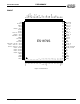
PRELIMINARY ES1879 DATA SHEET PINOUT 77 78 79 80 81 82 83 84 85 86 87 ES1879S 88 89 90 91 92 93 94 95 96 97 98 99 51 52 54 55 56 57 53 50 49 48 47 46 45 44 43 42 41 40 39 38 37 36 35 34 33 32 31 30 29 28 27 26 1 2 3 4 5 6 7 8 9 10 11 12 13 14 15 16 17 18 19 20 21 22 23 24 25 100 58 59 60 61 62 63 64 65 66 67 68 69 70 71 72 73 76 PCSPKO AOUT_R AOUT_L LINE_R LINE_ L CIN_R CIN_L FOUT_L FOUT_R VDDA CAP3D GNDA MIC CMR AUXA_R AUXA_L AUXB_R/FDXO AUXB_L/FDXI TA TB TC TD S WA SWB SWC
PRELIMINARY ES1879 DATA SHEET PIN DESCRIPTION PIN DESCRIPTION Name GNDD A[11:0] AEN VDDD D[7:0] SW(A-D) T(A-D) AUXB_L FDXI AUXB_R FDXO AUXA_L, AUXA_R CMR MIC GNDA CAP3D VDDA FOUT_L, FOUT_R CIN_L, CIN_R LINE_L, LINE_R AOUT_L, AOUT_R PCSPKO XA[3:0] Number 1, 24, 61, 78 13:2 14 15, 74, 100 23:16 28:25 32:29 I/O I I I I I/O I I/O Description Digital ground. ISA address bus. ISA address valid when active-low, DMA when high. Digital power supply (3.0 - 5.5 V). ISA data bus. 24 mA drivers.
PRELIMINARY ES1879 DATA SHEET PIN DESCRIPTION Name SECS Number 71 I/O I DOCKED 72 I RESET XI XO PCSPKI GPI0 DRQD GPI1 GPO[1:0] GPO2 SECLK DRQC GPI2 DACKBC GPI3 DRQB DACKBB DRQA DACKBA DACKBD MUTE GPI4 SEDI VOLUP GPI5 SEDO VOLDN GPI6 IRQE GPO6 IRQD GPO5 IRQC GPO4 IRQB GPO3 IRQA IORB IOWB 73 75 76 77 79 I I O I I O/Hi Z I O O I O/Hi Z I I I O/Hi Z I O/Hi Z I I I I I I I O I I O/Hi Z O O/Hi Z O O/Hi Z O O/Hi Z O O/Hi Z I O 80 82:81 83 84 85 86 87 88 89 90 91 92 93 94 95 96 97 98 99 ESS Technolog
PRELIMINARY ES1879 DATA SHEET FUNCTIONAL DESCRIPTION FUNCTIONAL DESCRIPTION This section shows the overall structure of the ES1879 and discusses its major functional subunits. GNDD The major subunits of the ES1879 are shown in Figure 2 and are briefly described in the following paragraphs.
PRELIMINARY ES1879 DATA SHEET FUNCTIONAL DESCRIPTION ESFM™ music synthesizer – high-quality OPL3 superset FM synthesizer. 3-D Processor – Spatializer technology 3-D audio effects Recording source and input volume control – input source and volume control for record. The recording source can be selected from one of seven choices: – Mic processor.
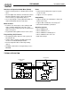
PRELIMINARY ES1879 DATA SHEET MIXER SCHEMATIC BLOCK DIAGRAM MIXER SCHEMATIC BLOCK DIAGRAM ADC/DAC DMA 1 Output Volume digital audio DAC DMA 2 digital audio DAC I2S/ZV I2S/ZV MPEG audio Preamp MIC Playback Mixer LINE Spatializer 3-D DOCKED On DAC FM/ HWWT ES978 Off AUXA Record Monitor Off AUXB Record Source ES978 ES978 Volume On Σ Mute Master Volume AOUT Σ Record Volume Input Volume ADC Record Mixer Mute Figure 3 ES1879 Mixer Schematic Block Diagram 10 SAM0025A-062397 ESS T
PRELIMINARY ES1879 DATA SHEET TYPICAL APPLICATION TYPICAL APPLICATION ISA BUS ES1879 2 or 3 Buttons Up, Down, and Mute ISA Bus Interface AOUT Stereo DSP Serial Port 3-D Processor Hardware Volume Control Joystick Controls CD (stereo) Aux B (stereo) Line (stereo) Mic (mono) L R Speakers 1-Mbyte Wavetable ROM ES981 MPU-401 2 MIDI Serial Port Wavetable Audio Port 2 Serial Port General MIDI Interpreter Wavetable Synthesizer Chorus & Reverb (ES69x only) ES689/ES69X I2S ZV MPEG Audio (I2
PRELIMINARY ES1879 DATA SHEET ISA BUS INTERFACE ISA BUS INTERFACE Table 1 shows the pins used to interface the ES1879 with the ISA bus. Table 1 ES1879 ISA Bus Interface Pin I/O A[11:0] I AEN I Description ISA address bus. ISA address valid when active-low, DMA when high. D[7:0] I/O ISA data bus. 24 mA drivers. IOWB O ISA active-low write strobe. IORB I ISA active-low read strobe. IRQ(A-E) O/Hi Z ISA interrupt request. 16 mA driver. I ISA active-low DMA acknowledge.
ES1879 DATA SHEET PRELIMINARY DIGITAL AUDIO Data Transfers in Compatibility Mode The first audio channel can be programmed using the standard Sound Blaster-compatible commands. These commands are written to the chip through port Audio_Base+Ch. When programming the first audio channel for Compatibilty mode transfers one of the following modes can be used: Direct Mode DMA Mode – Normal – Auto-Initialize In addition, both Normal DMA mode and Auto-Initialize DMA mode can use a special High-Speed mode.
PRELIMINARY ES1879 DATA SHEET DIGITAL AUDIO DMA Mode Extended mode DMA supports both Normal and AutoInitialize mode. In addition, Normal mode and AutoInitialize mode both support Single and Demand transfer modes. Using Single transfer, one byte is transferred per DMA request. Demand transfer reduces the number of DMA requests necessary to make a transfer by allowing two or four bytes to be transferred per DMA request. Thus there are multiple DMA acknowledges for each DMA request.
PRELIMINARY ES1879 DATA SHEET DRQ LATCH FEATURE A pop may be heard if the DAC level was left at a value other than mid-level (code 80h on an 8-bit scale) by the previous play operation. To prevent this, always finish a DAC transfer with a command to set the DAC level to midrange: 10h + 80h DRQ LATCH FEATURE The DRQ latch feature is enabled when bit 7 of VendorDefined Card-Level register 29h is high (see Figure 6).
PRELIMINARY ES1879 DATA SHEET INTERRUPTS INTERRUPTS There are four interrupt sources in the ES1879: Table 2 ES1879 Interrupt Sources Interrupt Source Description Audio 1 This interrupt is used for the first audio channel (Sound Blaster-compatible DMA, Extended mode DMA, and Extended mode Programmed I/O), as well as SB-compatible (Sound Blaster-compatible) MIDI receive. This interrupt request is cleared by a hardware or software reset, or by an I/O read from Audio_Base+Eh.
ES1879 DATA SHEET PRELIMINARY INTERRUPTS A second use of the IMR is within an interrupt handler. The first thing the interrupt handler can do is mask all of the interrupt sources mapped to the interrupt handler. The ISR can then be polled to decide which sources to process. Just before exiting the interrupt handler, the IMR can be restored.
PRELIMINARY ES1879 DATA SHEET PERIPHERAL INTERFACING PERIPHERAL INTERFACING DSP Interface Telegaming Mode The ES1879 contains a synchronous serial interface for connection to a DSP serial interface. The typical application for this interface is a speakerphone. This mode is enabled when two conditions are present: Table 3 DSP Interface Pins Bit 0 of mixer register 48h is high. This bit enables The DSP serial port must be enabled (i.e., bit 7 of Mixer register 48h is high). Telegaming mode.
PRELIMINARY ES1879 DATA SHEET PERIPHERAL INTERFACING DSP Digital Audio Playback Mixing External to the ES1879 There are two choices for mixing the DSP digital audio playback data with other audio sources. The audio data can be mixed in the ES1879’s internal playback mixer or external to the ES1879. The second method is to use the FDXO output pin and mix the DSP digital audio playback and the game-compatible digital audio playback in an external audio mixer.
PRELIMINARY ES1879 DATA SHEET PERIPHERAL INTERFACING I2S Serial Interface Three input pins, IIDATA, IISCLK, and IILR, are used for a serial interface between an external device and a stereo DAC within the ES1879. IIDATA, IISCLK, and IILR can be left floating or connected to ground if the serial interface is not used. 2 A typical applications of the I S serial interface is MPEG audio or CD audio. I2S Serial Interface Timing This section discusses the I2S serial interface signals.
ES1879 DATA SHEET PRELIMINARY PERIPHERAL INTERFACING Game/Joystick Interface The ES1879 includes 8 pins for a dual joystick port. The digital game port address is decoded for timer pins TA, TB, TC, and TD, and for switch pins SWA, SWB, SWC, and SWD. The MIDI serial input and output also come from the game port connector in most applications. Four of these eight pins, SW(A-D), are inputs switches of the joysticks.
PRELIMINARY ES1879 DATA SHEET PERIPHERAL INTERFACING JOYSTICK PORT 8 15 7 14 6 13 5 12 4 11 3 10 2 9 1 R3 220 R4 2.2K R1 10K Q1 2N3904 R2 270 Q2 2N3904 R5 5.6K C1 220pF C2 220pF 5 3 2 4 1 DIN J1 MIDI OUT R6 270 D1 DB15P ISO1 5 3 MIDI IN 2 4 1 DIN J2 Figure 11 MIDI Serial Interface Adapter ES978 Interface When docked, the ES1879 is in constant communication with the ES978 in the expansion unit. A half-duplex, bidirectional serial link keeps each chip updated on the status of the other.
PRELIMINARY ES1879 DATA SHEET PERIPHERAL INTERFACING Table 9 shows the mode configurations when the notebook unit is docked. Table 9 Docked Modes for Analog Audio Mode XA0 XA1 XA2 XA3 0 -Left Play +Left Play -Right Play +Right Play 1 +Left Record -Left Record +Right Record -Right Record 2 -Play +Play +Record -Record 3 Left Record Left Play Right Record Right Play Docking Status The ES1879 is either in docked or undocked state.
PRELIMINARY ES1879 DATA SHEET PERIPHERAL INTERFACING Audio_Base+7h. Only bit 5 (FM reset) and bit 7 (suspend request) of I/O port Audio_Base+7h are supported in the ES1879. Expansion Audio Interface – Digital Two wires are used to transmit serial data between the ES1879 and ES978. The first signal, XSC, acts as a frame sync and shift clock. The bit clock rate is 3.58 MHz. Table 10 contains the data configuration for the download period.
ES1879 DATA SHEET PRELIMINARY PERIPHERAL INTERFACING Table 11 contains the data configuration for the upload period. Table 11 Upload Period Data Configuration Byte 0 Bits Function 3:0 4 5 6 7 Joystick switch status VOLUP input status VOLDN input status MUTE input status 1: MIDI receive data following 1 15:8 MIDI receive data if bit 7 of byte 0 is set.
PRELIMINARY ES1879 DATA SHEET PERIPHERAL INTERFACING The amount of effect can be controlled by either directly programming mixer register 52h or by allowing the ES1879 to control the effect level automatically, based on the stereo content of the input signal. This latter feature is called auto-limiting. In auto-limiting, the ES1879 constantly adjusts the amount of effect based on the stereo content of the input signal. The host software can set a maximum effect level by programming register 52h.
PRELIMINARY ES1879 DATA SHEET PERIPHERAL INTERFACING Split Mode Normally, the hardware volume controls change the master volume registers directly and produce an interrupt at each change. Instead, the ES1879 can be programmed to use Split mode. In this case, the hardware volume counters (mixer registers 61h and 63h) are split from the master volume registers (mixer registers 60h and 62h). Pressing a hardware volume control button changes the hardware volume counter and produces an interrupt.
PRELIMINARY ES1879 DATA SHEET ANALOG DESIGN CONSIDERATIONS ANALOG DESIGN CONSIDERATIONS This section describes design considerations related to inputs and outputs of analog signals and related pins on the chip. Reference Generator Reference generator pin CMR is connected through bypass capacitors to analog ground.
ES1879 DATA SHEET PRELIMINARY CONFIGURATION CONFIGURATION The ES1879 supports the industry-standard ISA Plug and Play (PnP) specification, as well as a software configuration method that does not rely on PnP. Bit 2 of PnP vendor register 2Dh determines the configuration method. When bit 2 is high, the ISA PnP configuration mode is disabled. Bit 2 is low (ISA PnP) by default. NOTE: The ES1878 supported PnP from an internal ROM and/or a bypass key. External EEPROM was not supported.
PRELIMINARY ES1879 DATA SHEET CONFIGURATION Accessing the ROM/EEPROM EEPROM Function Action Read EEPROM data register or read internal ROM, then increment one address. Read PnP Vendor register 2Eh. Write EEPROM data register, then increment one address. Write PnP Vendor register 2Eh. Write EEPROM command register. Write PnP vendor register 2Fh. Reset EEPROM/ROM address counter. Read PnP vendor register 2Fh.
ES1879 DATA SHEET PRELIMINARY CONFIGURATION Example Using Non PnP Method to Configure the ES1879: 1. Enable the configuration device at I/O address 800h by sending the bypass key with interrupts disabled. 2. Program Vendor-Defined Card-Level registers 20h2Dh as follows: write Vendor-Defined Card-Level register number to I/O address 800h and data to I/O address 801h. 1. 20h, 21h, 22h: assign ISA IRQ channels to pins. Unused pins are assigned to IRQ1. 2. 23h, 24h: assign ISA DMA channels to pins.
PRELIMINARY ES1879 DATA SHEET CONFIGURATION Card-Control Card-Level Registers (00h – 07h) This section describes the PnP Card registers of the ES1879. Resource Data Set RD_DATA Port Returns next byte of resource data, provided the status bit in register 05h has been polled before each byte read, indicating that data is ready. Only works in Configuration mode. (00h, R/W) Bits 9:2 of the PnP RD_DATA port 7 6 5 4 3 2 1 0 The PnP read port can be written only when the card is in Isolation mode.
PRELIMINARY ES1879 DATA SHEET CONFIGURATION Vendor-Defined Card-Level Registers (20h – 2Fh) This section describes the PnP Vendor registers of the ES1879. IRQB, IRQA MPU-401 LDN 1/ LDN 3 x 7 6 (20h, R) IRQB 7 Shared Function Assignment 6 IRQA 5 4 3 2 VOLUP, MUTE/ VOLDN/ GPI4 GPI5, GPI6 5 4 (25h, R) IRQE/ GPO6 IRQD/ GPO5 IRQC/ GPO4 IRQB/ GPO3 3 2 1 0 Loaded from Configuration ROM header after PnP reset. 1 0 Bit Definitions: Defines IRQ number assigned to B and A pins.
PRELIMINARY ES1879 DATA SHEET CONFIGURATION GPI Map (27h, R) x GPI6 GPI5 GPI4 GPI3 GPI2 GPI1 GPI0 7 6 5 4 3 2 1 0 One bit for each GPI[6:0]. This register is reset to zero by hardware reset but not by PnP reset.
PRELIMINARY ES1879 DATA SHEET CONFIGURATION Miscellaneous Analog Control External record volume 7 (2Bh, R) ES978 ES1879 ES1879 master 2 ES978 mappable I S volume I2S volume volume mute mixer target tracking control 6 5 4 3 2 1 0 The I2S DAC volume can track the volume of the FM DAC when its own Mixer Volume Control register 6Dh is not used. This is useful when the I2S interface is used for an external wavetable synthesizer.
PRELIMINARY ES1879 DATA SHEET CONFIGURATION Power Management (2Dh, R/W) IPROM PnP state disable flag x 7 6 5 4 3 2 Table 13 Logical Device Summary Power 1 Logical Device Registers 0 After hardware reset or PnP reset, this register is set to 03h. Suspend and Resume operation requires programming register Audio_Base+7h. LDN # Device LDN 0 (mandatory) Configuration device 30h Activate; bit 0 is activate bit. 31h I/O Range Check. 60h I/O base address, bits 11:8.
PRELIMINARY ES1879 DATA SHEET CONFIGURATION LDN 0: Configuration Device Activate (30h, R/W) 0 7 6 5 Activate 4 3 2 1 0 After reset or after a 1 is written to the reset bit in the card’s configuration control bit, the default for this register is 0. LDN 1: Audio Device This device actually supports three functions: audio, FM, and MPU-401. Audio requires sixteen I/O locations, one interrupt that is shared with MPU-401, and two DMA channels. FM requires four I/O locations.
PRELIMINARY ES1879 DATA SHEET CONFIGURATION FM Alias I/O Base Address (62h, R/W) 0 7 6 A[11:8] 5 4 3 2 1 0 I/O base address of FM alias, bits 11:8. Four locations. FM Alias I/O Base Address 6 5 0 0 0 0 0 0 1 0 7 6 5 4 3 2 1 0 Interrupt request type select 1. Returns 2 (low-to-high transition). DMA Channel Select 0 0 4 (73h, R) (63h, R/W) A[7:2] 7 Interrupt Request Type Select 1 3 2 1 (74h, R) 0 0 7 6 5 Data 4 3 2 1 0 I/O base address of FM alias, bits 7:2.
PRELIMINARY ES1879 DATA SHEET CONFIGURATION LDN 2: Joystick Device Activate (30h, R/W) 0 7 6 5 LDN 3: MPU-401 Device The MPU-401, as an independent device, is optional; normally MPU-401 is part of the AudioDrive® solution. Activate 4 3 2 1 0 Activate (30h, R/W) 0 After reset or after a 1 is written to the reset bit in the card’s configuration control bit, the default for this register is 0. Bits Name Description 7:1 Reserved. Always write 0. 0 Activate 1 = Activate.
PRELIMINARY ES1879 DATA SHEET CONFIGURATION Interrupt Request Level Select 0 (70h, R/W) 0 7 6 Data 5 4 3 2 1 0 Interrupt request level select 0. Bit Definitions: Bits Name Description 7:4 Reserved. Always write 0. – 3:0 Data Select which interrupt level used for Interrupt 0. Interrupt Request Type Select 0 (71h, R) 0 0 0 0 0 0 1 0 7 6 5 4 3 2 1 0 Interrupt request type select 0. Returns 2 (low-to-high transition). 40 SAM0025A-062397 ESS Technology, Inc.
PRELIMINARY ES1879 DATA SHEET I/O PORTS I/O PORTS Table 14 I/O Ports for Configuration, Audio, FM, MPU-401, and Joystick Devices Port Read/Write Function Base+0h Read/write Configuration Register Address. Base+1h Read/write Configuration Register Data. Base+2h Read/write ES1879 GPO State register. Base+3h Read/write ES978 GPO State register. Base+4h Read-only ES1879 GPI Status register. Base+5h Read-only ES978 GPI Status register. Base+6h Read-only Interrupt Status register.
PRELIMINARY ES1879 DATA SHEET I/O PORTS ES978 GPO State Register (Config_Base+3h, R/W) x GPO6 GPO5 GPO4 GPO3 GPO2 GPO1 GPO0 7 6 5 4 3 2 1 0 Sets the state of the ES978 GPO pins that are not mapped to GPI pins of the ES1879.
PRELIMINARY ES1879 DATA SHEET I/O PORTS Audio Device Reset and Status Flags Mixer Address Register (Audio_Base+4h, R/W) x A6 A5 A4 A3 A2 A1 0 7 6 5 4 3 2 1 0 The ES1879 provides a means to read back the Mixer Address register. Reading back this register is useful for a “hot-key” application that needs to change the mixer while preserving the address register.
PRELIMINARY ES1879 DATA SHEET I/O PORTS Power Management Register Suspend request 0 FM synth reset 7 6 5 (Audio_Base+7h, R/W) 0 4 3 2 1 0 Reading or writing port Audio_Base+7h does not automatically wake up the ES1879. Bit Definitions: Bits Name 7 6 5 4:0 Read Data Register D7 D6 D5 D4 D3 D2 D1 D0 7 6 5 4 3 2 1 0 Bit Definitions: Bits Name 7 6 1 = Data available in read buffer. 0 = Data not available in read buffer. This flag is reset by a read from port Audio_Base+Ah.
PRELIMINARY ES1879 DATA SHEET I/O PORTS FM Device The FM synthesizer operates in two different modes: Emulation mode and Native mode. In Emulation mode, the FM synthesizer is fully compatible with the OPL3 FM synthesizer. In Native mode, the FM synthesizer has increased capabilities and performance for more realistic music. The following register descriptions are for Emulation mode only.
PRELIMINARY ES1879 DATA SHEET I/O PORTS Joystick Device The joystick device uses only a single I/O port. The device can function in one of two modes: Analog mode or Digital mode. The use of this I/O port is different depending on the mode. This section describes Analog mode. Digital mode is described in the MPU-401/Joystick Interface section. Joystick_Base+0h (W) x x x x x x x x 7 6 5 4 3 2 1 0 Any value written to the Joystick_Base+0h port will restart the timing sequence.
ES1879 DATA SHEET PRELIMINARY PROGRAMMING THE ES1879 PROGRAMMING THE ES1879 Identifying the ES1879 The ES1879 can be identified by reading Mixer Extension register 40h successfully. Mixer Extension register 40h returns the following 8-bit values on four successive reads: 18h, 79h, A[11:8], A[7:0] where 18h and 79h are data reads indicating the part number (1879) and A[11:0] is the base address of the configuration device.
PRELIMINARY ES1879 DATA SHEET PROGRAMMING THE ES1879 Table 15 Comparison of Operation Modes Compatibility Mode (Sound Blaster Pro) Extended Mode Sound Blaster Pro-compatible Yes No FIFO size 64 bytes (firmware managed) 256 bytes (hardware managed) Mono 8-bit ADC, DAC Yes, to 44 kHz Yes, to 44 kHz Mono 16-bit ADC, DAC Yes, to 22 kHz Yes, to 44 kHz Stereo 8-bit DAC Yes, to 22 kHz Yes, to 44 kHz Stereo 8-bit ADC Yes, to 22 kHz Yes, to 44 kHz Stereo 16-bit DAC Yes, to 11 kHz Yes, to 44 k
PRELIMINARY ES1879 DATA SHEET PROGRAMMING THE ES1879 For 16-bit data, the ES1879 expects DMA transfers to be a multiple of 4, with repeating groups in the order: 1. Left low byte 2. Left high byte 3. Right low byte 4.
PRELIMINARY ES1879 DATA SHEET PROGRAMMING THE ES1879 Compatibility Mode Programming This section describes Compatibility mode programming. Compatibility Mode DAC Operation 1. Reset 7. Delay approximately 100 milliseconds to allow the analog circuits to settle, then enable the Audio 1 DAC input to mixer with command D1h. 8. During DMA. Write 1h to port Audio_Base+6h.
ES1879 DATA SHEET PRELIMINARY PROGRAMMING THE ES1879 Compatibility Mode ADC Operation ES1879 analog circuitry is switched from the DAC direction to the ADC direction by the first direct or DMA mode ADC command (2xh). Discard the first 25 to 100 milliseconds of samples because pops might occur in the data due to the change from the DAC to ADC direction. In the ADC direction, the digital audio input to the mixer is automatically muted. 1. Reset Write 1h to port Audio_Base+6h.
PRELIMINARY ES1879 DATA SHEET PROGRAMMING THE ES1879 The maximum sample rate for Direct mode ADC is 22 kHz. A4h, 00h; register A4h = 00h The maximum sample rate for DMA ADC for both 8-bit and 16-bit is 22 kHz, using commands 24h, 25h, 2Ch, or 2Dh. A5h, F8h; register A5h = F8h There is a special High-Speed mode for ADC that allows 8-bit sampling up to 44 kHz. This mode uses commands 98h (auto-initialize) and 99h (normal). No AGC is performed as the input volume is controlled with command DDh.
ES1879 DATA SHEET PRELIMINARY PROGRAMMING THE ES1879 Extended Mode Audio 1 DAC Operation Follow the steps below to program the first audio channel for Extended mode DAC operation. 1. Reset: Write 3h to port Audio_Base+6h, instead of 1h as in Compatibility mode. Bit 1 high specifically clears the FIFO. The remainder of the software reset is identical to Compatibility mode. Reset disables the Audio 1 DAC input to the mixer. This is intended to mask any pops created during the setup of the DMA transfer. 2.
PRELIMINARY ES1879 DATA SHEET PROGRAMMING THE ES1879 For Normal mode, initialize the system DMA controller with the address and count of the next block to transfer. Update the ES1879 Transfer Count registers if the count is changed. To start the next transfer, clear bit 0 of register B8h, then set it high again. To stop a DMA transaction in progress, clear bit 0 of register B8h.
PRELIMINARY ES1879 DATA SHEET PROGRAMMING THE ES1879 14.After DMA is finished: Table 19 Command Sequences for DMA Record Mono Stereo 8-bits 16-bits Unsigned Signed X X X X X X X X X X X X X Reg B7h = 51h Reg B7h = D0h X X X X X Reg B7h = 71h Reg B7h = F4h Reg B7h = 51h Reg B7h = 98h X X Reg B7h = 71h Reg B7h = F0h Reg B7h = 51h Reg B7h = D4h X X Sequence X Reg B7h = 71h Reg B7h = B8h Reg B7h = 51h Reg B7h = 9Ch X Reg B7h = 71h Reg B7h = BCh 9.
PRELIMINARY ES1879 DATA SHEET PROGRAMMING THE ES1879 NOTE: The ES1879 is designed for I/O block transfer up to an ISA bus speed of 8.33 MHz. Programmed I/O DAC Operation Programmed I/O DAC operation is done just as explained under “Extended Mode Audio 1 DAC Operation” on page 53 with the following exceptions: 3. Program transfer type: register 78h: Register 78h: Set bit 4 low for Normal DMA mode, high for Auto-Initialize DMA mode. Bits 7:6 01: Demand transfer DMA: 2 bytes per DMA request.
ES1879 DATA SHEET PRELIMINARY PROGRAMMING THE ES1879 To stop a DMA transaction in progress, clear bit 0 of register B8h. To stop a DMA transaction after the current auto-initialize block is finished, clear bit 4 of register 78h, wait for the interrupt, and then clear bits 1:0 of register 78h. 11. After DMA is finished: Restore the system interrupt controller and DMA controller to their idle state. Monitor the FIFO Empty status flag in port Audio_Base+Ch to be sure data transfer is completed.
PRELIMINARY ES1879 DATA SHEET PROGRAMMING THE ES1879 6. Program transfer type: register 78h: Register 78h: Set bit 4 high for Auto-Initialize DMA mode. Bits 7:6 00: Single transfer DMA. 01: Demand transfer DMA: 2 bytes per DMA request. 10: Demand transfer DMA: 4 bytes per DMA request. 11: Demand transfer DMA: 8 bytes per DMA request. 7. Clocks and counters: registers 70h, 72h, 74h, and 76h: Set the sample rate the same as in A1h. Set the Transfer Count Reload to 64 bytes.
PRELIMINARY ES1879 DATA SHEET PROGRAMMING THE ES1879 Programming the ES1879 Mixer The ES1879 has a set of mixer registers that are backward compatible with the Sound Blaster Pro. However, some of the registers have an “extended” or “alternate” way of accessing the registers to provide for greater functionality. Commanding the ES1879 Mixer Registers There are two I/O addresses used by the mixer: Audio_Base+4h is the address port; Audio_Base+5h is the data port.
PRELIMINARY ES1879 DATA SHEET PROGRAMMING THE ES1879 Extended Access to ADC Source Select In Sound Blaster Compatibility mode in the Sound Blaster Pro mixer, there are three choices for recording source, set by bits 2 and 1 of Mixer register 0Ch.
PRELIMINARY ES1879 DATA SHEET PROGRAMMING THE ES1879 Table 21 Mixer Input Volume Registers If Sound Blaster Pro volume emulation is enabled, then a mixer reset will cause both left and right channels to set to their power-on default, namely 54 (or 36h).
PRELIMINARY ES1879 DATA SHEET REGISTERS REGISTERS Types of Register Access There are two types of audio registers in the ES1879: Mixer registers These registers are accessed via I/O ports Audio_Base+4h and Audio_Base+5h. Audio_Base+4h is written with the register address. Then the register can be read/written via Audio_Base+5h. These registers control many functions other than the mixer.
PRELIMINARY ES1879 DATA SHEET REGISTERS ESS Mixer Registers This section provides a summary of the ESS mixer registers followed by a detailed description of each register.
PRELIMINARY ES1879 DATA SHEET REGISTERS Table 25 ESS Mixer Register Summary (Continued) Reg D7 D6 D5 D4 65h D3 D2 D1 Remark Opamp calibration 0 66h D0 Opamp calibration control Write: Reset hardware volume interrupt request 67h ES978 mix volume ES978 record mixer tracking mode select ES978 mix into playback 0 Hardware volume interrupt request Interface mode select ES978 interface mode control 68h Mic mix volume left Mic mix volume right Mic record volume 69h Audio 2 volume left
PRELIMINARY ES1879 DATA SHEET REGISTERS Record Source Select (1Ch, W) x x F1 x F0 7 6 5 4 3 Record Source 2 1 Bits Definitions: Description 7:6 – No function. 5 F1 Sound Blaster Pro filter control bit. Has no function in the ES1879 and is ignored. 4 – No function. 3 F0 Sound Blaster Pro filter control bit. Has no function in the ES1879 and is ignored.
PRELIMINARY ES1879 DATA SHEET REGISTERS PC Speaker Volume (3Ch, R/W) PC speaker volume 7 6 5 4 3 2 1 0 Serial Interface Registers This section describes registers related to the DSP and ES689/ES69x serial interface. This register controls the PC speaker volume. Bits 2:0 select the attenuation level in steps of -3 dB. The maximum setting of 08h corresponds to 0 dB attenuation. On reset, this register assumes the value of 04h.
PRELIMINARY ES1879 DATA SHEET REGISTERS Serial Mode Output Control Output override 7 (44h, R/W) Output signal 6 5 Output volume 4 3 2 1 0 Serial Mode Miscellaneous Analog Control (46h, R/W) Analog Music control mixer override test 7 6 Left ADC Right ADC Mono enable x FDXO enable FDXI enable 5 4 3 2 1 0 Bits Definitions: Bits Name 7 Output override 6:4 Output signal 3:0 Output volume Description 1 = Output volume during serial mode is from this register rather than from the Mixer
PRELIMINARY ES1879 DATA SHEET REGISTERS Serial Mode Miscellaneous Control Serial Data enable format 7 (48h, R/W) ES689/ DSP Serial ES69x Active test reset interface low sync mode enable 6 5 4 3 2 7 68 (4Ah, R/W) 0 0 Telegaming mode enable 1 0 Bits Definitions: Bits Name FS Rate Control Description Serial enable 1 = Enable DSP serial port. This signal is synchronized with DCLK input rising edge. If DCLK is not running, enabling Serial enable has no effect. 0 = Disable DSP serial port.
PRELIMINARY ES1879 DATA SHEET REGISTERS Serial Mode Filter Divider Control Filter override 7 0 6 5 (4Ch, R/W) 2’s complement filter divider 4 3 2 1 0 This register controls the filter clock rate during serial mode. Bits Definitions: Bits Name 7 Filter override Description 1 = During serial mode, the filter clock is generated by dividing down the serial clock.
PRELIMINARY ES1879 DATA SHEET REGISTERS Spatializer Audio Processor Registers Spatializer Auto-Limit Scale Factor 2 This section describes registers related to the Spatializer 3-D audio processor. Spatializer Enable and Mode Control 0 0 0 0 7 6 5 4 (50h, R/W) Spatializer enable Reset Mono mode Auto-limit 3 2 1 0 Reset to zero by hardware reset. 3 1 Mono mode 1 = Mono-in, stereo-out mode. 0 = Stereo-in, stereo-out mode.
PRELIMINARY ES1879 DATA SHEET REGISTERS Spatializer Test Control Left/Right state flag (5Ch, R/W) Accelerated Signal Auto-Limit ADC test timing processor test mode mode enable test mode 7 6 5 4 THD flag Down flag Up flag 2 1 0 3 In ADC or signal processor test mode, four reads or writes are needed to access all four bytes. The sequence is controlled by an internal 2-bit counter. This counter is incremented after every I/O read or write to mixer register 5Eh.
PRELIMINARY ES1879 DATA SHEET REGISTERS Extended Mode Master Volume Control Registers Right Master Volume and Mute This section describes registers related to the master volume control in Extended mode. These registers are accessed via I/O addresses Audio_Base+4h and Audio_Base+5h. Left Master Volume and Mute 0 Mute 7 6 (60h, R/W) Left master volume 5 4 3 2 1 0 This register determines the master volume level for the left channel.
PRELIMINARY ES1879 DATA SHEET REGISTERS Master Volume Control (64h, R/W) SB Pro HWV Split master MPU-401 Volume HWV HWV operainterrupt mode volume IRQ mask count IRQ flag tion mode mask enable disable 7 6 5 4 3 2 1 Bits Name 0 0 Description SB Pro master volume disable When low, a write to legacy master volume registers 22h or 32h is translated into a write to the hardware master volume counters, Mixer registers 60h and 62h.
PRELIMINARY ES1879 DATA SHEET REGISTERS ES978 Interface Mode Control (67h, R/W) ES978 mix volume 0 ES978 audio mix into playback enable ES978 record mixer tracking mode select 7 4 3 2 6 5 Interface mode select 1 0 In the ES1878, the mode of the interface to the ES978 (playback vs record, mono vs full-duplex) was determined by the state of the CODEC inside the ES1878 automatically. In the ES1879, the mode of the interface is determined by mixer register 67h.
PRELIMINARY ES1879 DATA SHEET REGISTERS I2S Record Volume (6Fh, R/W) I S record volume left 7 6 5 Audio 1 and Audio 2 Mode I S record volume right 2 2 4 3 2 1 0 This register controls the record volume for the I2S input. Set low by hardware reset but not by mixer reset.
PRELIMINARY ES1879 DATA SHEET REGISTERS Audio 2 Filter Clock Divider (72h, R/W) Filter clock divider 7 6 5 4 3 2 1 0 This register controls the low-pass frequency of the switch-capacitor filters inside the ES1879. Generally, the filter roll-off should be positioned at 80% - 90% of the Sample_Rate/2 frequency. The ratio of the roll-off frequency to the filter clock frequency is 1:82.
PRELIMINARY ES1879 DATA SHEET REGISTERS Audio 2 Control 2 IRQ IRQ mask latch 7 (7Ah, R/W) 0 6 5 4 3 FIFO signed mode FIFO stereo mode FIFO 16-bit mode 2 1 0 Audio 2 Configuration Mic preamp enable 0 7 6 (7Dh, R/W) 5 4 3 FDXO source select 2 1 This register is reset to zero by hardware or software reset. This register is reset to 08h by hardware reset. Bits Definitions: Bits Definitions: Bits Name 7 6 5:3 Description IRQ latch Audio 2 Interrupt Request Latch.
PRELIMINARY ES1879 DATA SHEET REGISTERS Test Register (7Eh, R/W) ADC test Test bus MIDI loop- FM test enable enable back test enable DSP loopback test 2nd DMA test enable 0 2 1 0 Table 26 Test Bus Assignments SEL[3:0] TST[7:0] in Test Mode 1 TST[7:0] in Test Mode 2 0 DAC/ADC1 data left [7:0] DAC2 data left [7:0] 1 DAC/ADC1 data left [15:8] DAC2 data left [15:8] This register is a test register.
PRELIMINARY ES1879 DATA SHEET REGISTERS Controller Registers This is a summary and description of the controller registers. These registers are written to and read from using commands of the format Axh or Bxh. To enable access to these registers, send the command C6h.
PRELIMINARY ES1879 DATA SHEET REGISTERS Audio 1 Filter Clock Divider (A2h, R/W) Filter clock divider 7 6 5 4 3 2 1 Analog Control 0 0 0 1 Record monitor enable 0 7 6 5 4 3 2 0 This register controls the low-pass frequency of the switch-capacitor filters inside the ES1879. Generally, the filter roll-off should be positioned at 80%-90% of the Sample_Rate/2 frequency. The ratio of the roll-off frequency to the filter clock frequency is 1:82.
PRELIMINARY ES1879 DATA SHEET REGISTERS Legacy Audio Interrupt Control Enable IRQ for GameEnable IRQ ovf Ext FIFO1 HE status compatible mode DMA cntr edge IRQ 7 6 Bit Definitions: Bits Name 5 (B1h, R/W) x Audio 1 interrupt 4 3 2 1 0 Description 7 Game-com- Reserved for Compatibility mode. Leave zero patible IRQ for Extended mode. 6 Enable Set high to receive interrupts for each overIRQ ovf Ext flow of the ES1879 DMA counter in Extended mode DMA mode.
PRELIMINARY ES1879 DATA SHEET REGISTERS Record Level (B4h, R/W) Left channel record level 7 6 5 Right channel record level 4 3 2 1 0 Register B4h allows for independent left and right record levels. Each channel has 16 levels (excluding mute). The amount of gain or attenuation for each level is different for microphone than for all other sources. The record levels are listed in the following table.
PRELIMINARY ES1879 DATA SHEET REGISTERS Audio 1 Transfer Type (B9h, R/W) 0 7 6 5 4 Bit Definitions: Bits Name 7:2 DMA transfer type select 3 2 1 0 Description – Reserved. Always write 0.
PRELIMINARY ES1879 DATA SHEET AUDIO MICROCONTROLLER COMMAND SUMMARY AUDIO MICROCONTROLLER COMMAND SUMMARY Table 28 Command Summary Command Data Byte(s) Write/Read Function 10h 1 write Direct write 8-bit DAC. Data is 8-bit unsigned format. 11h 2 writes Direct write 16-bit DAC. Data is 16-bit unsigned format, first low byte then high byte. 14h 2 writes Start Normal mode DMA for 8-bit DAC transfer. Data is transfer count-1, least byte first.
PRELIMINARY ES1879 DATA SHEET AUDIO MICROCONTROLLER COMMAND SUMMARY Table 28 Command Summary (Continued) Command Data Byte(s) Write/Read 64h 2 writes Start ESPCM® 4.3-bit (low compression) format DMA transfer to DAC. Data is transfer count-1, least byte first. 65h 2 writes Same as command 64h, except with Reference Byte flag. 66h 2 writes Start ESPCM® 3.4-bit (medium compression) format DMA transfer to DAC. Data is transfer count-1, least byte first.
PRELIMINARY ES1879 DATA SHEET AUDIO MICROCONTROLLER COMMAND SUMMARY Table 28 Command Summary (Continued) Command Data Byte(s) Write/Read Function DCh 1 read Return current input gain, 0-15 (valid during 16-bit ADC and 8-bit “High-Speed mode” ADC). DDh 1 write Write current input gain, 0-15 (valid during 16-bit ADC and 8-bit “High-Speed mode” ADC). E1h 2 reads Return version number high (3), followed by version number low (1). This indicates Sound Blaster Pro compatibility.
ES1879 DATA SHEET PRELIMINARY POWER MANAGEMENT POWER MANAGEMENT Power management in the ES1879 is controlled by PnP Configuration register 2Dh. In previous AudioDrive® chips, power management was controlled by I/O port Audio_Base+7h. Only bit 5 (FM reset) and bit 7 (suspend request) of I/O port Audio_Base+7h are supported in the ES1879. GPO, XSD, and XSC are not affected during power-down. XA[3:0] are high-impedance during power-down Modes 0 and 1.
PRELIMINARY ES1879 DATA SHEET POWER MANAGEMENT ES1879 DRQ and IRQ lines are high-impedance. If a DRQ or IRQ line floats high, it can produce a false DMA cycle or interrupt. 88 SAM0025A-062397 ESS Technology, Inc.
PRELIMINARY ES1879 DATA SHEET ELECTRICAL CHARACTERISTICS ELECTRICAL CHARACTERISTICS The ES1879 is designed to operate at case temperatures of less than 78 °C. Absolute Maximum Ratings Rating Symbol Value Analog supply voltage range VDDA -0.3 to 7.0 V Digital supply voltage range VDDD -0.3 to 7.0 V Input voltage VIN -0.3 to 7.
PRELIMINARY ES1879 DATA SHEET ELECTRICAL CHARACTERISTICS Table 31 Analog Characteristics (VDDA = 5.0 V ± 5%; TA = 25 °C) (Continued) Pins Parameter MIC Input voltage range LINE_L, LINE_R, AUXA_L, AUXA_R, AUXB_L, AUXB_R Min Max Units 10 Typ 125 mVp-p 0.5 VDDA - 1.0 volts 3.5 Vp-p 0.5 VDDA - 1.0 volts FDXI AOUT_L, AOUT_R full-scale output range Output voltage range FDXO MIC Mic preamp gain 2.
PRELIMINARY ES1879 DATA SHEET ES1879 TIMING DIAGRAMS ES1879 TIMING DIAGRAMS t1 RESET Figure 18 Reset Timing AEN, A[11:0] t2 IORB t3 t4 D[7:0] t5 Figure 19 I/O Read Cycle AEN, A[11:0] t2 IOWB t3 t6 t7 D[7:0] Figure 20 I/O Write Cycle ESS Technology, Inc.
PRELIMINARY ES1879 DATA SHEET ES1879 TIMING DIAGRAMS DRQ t8 AEN t10 t11 DACKB t9 IOWB t12 t6 t7 D[7:0] Figure 21 Compatibility Mode DMA Write Cycle1 DRQ t10 AEN t11 t13 DACKB IORB t12 t5 D[7:0] t4 Figure 22 Compatibility Mode DMA Read Cycle 1. 92 In Compatibility mode DMA, the DMA request is reset by the acknowledge signal going low.
PRELIMINARY ES1879 DATA SHEET ES1879 TIMING DIAGRAMS DCLK t15 FS t16 t19 t16 DR D15 D14 D0 t15 t16 Figure 23 Serial Mode Receive Operation t20 DCLK t15 FS t16 t19 t18 DX D15 D14 D1 D0 t17 Figure 24 Serial Mode Transmit Operation ESS Technology, Inc.
PRELIMINARY ES1879 DATA SHEET ES1879 TIMING DIAGRAMS IILR t22 t21 t24 t23 IISCLK t25 t26 IIDATA Figure 25 Serial Input Timing for I2S Interface IISCLK LEFT IILR IIDATA R0* L15 L14 RIGHT L13 L12 L0 R15 R14 R13 R12 R11 R10 R0 * Note: LSB of right channel, previous sample. Figure 26 I2S Digital Input Format with 16 SCLK Periods 94 SAM0025A-062397 ESS Technology, Inc.
PRELIMINARY ES1879 DATA SHEET TIMING CHARACTERISTICS TIMING CHARACTERISTICS Symbol Parameter Min t1 Reset pulse width 300 Typ Max ns t2 IORB, IOWB pulse width 100 ns t3 IORB, IOWB address setup time 10 ns t4 Read data access time 70 ns t5 Read data hold time 10 ns t6 Write data setup time 5 ns t7 Write data hold time 10 ns t8 DMA request to AEN high 0 ns t9 DMA request to DMA ACK low 10 ns t10 DMA ACK to request release t11 DMA ACK high to AEN low 0 ns t12 D
PRELIMINARY ES1879 DATA SHEET MECHANICAL DIMENSIONS MECHANICAL DIMENSIONS D D1 A2 E E1 A1 ES1879 e L e1 b L1 1 Figure 27 ES1879 Physical Dimensions Symbol Description Millimeters Min Nom Max D Lead-to-lead, X-axis 15.75 16.00 16.25 D1 Package's outside, X-axis 13.90 14.00 14.10 E Lead-to-lead, Y-axis 15.75 16.00 16.25 E1 Package's outside, Y-axis 13.90 14.00 14.10 A1 Board standoff 0.05 0.10 0.15 A2 Package thickness 1.35 1.40 1.45 b Lead width 0.17 0.
ES1879 DATA SHEET PRELIMINARY APPENDIX A: ES1879 INTERNAL PNP RESOURCE ROM APPENDIX A: ES1879 INTERNAL PNP RESOURCE ROM ; system00.
PRELIMINARY ES1879 DATA SHEET APPENDIX A: ES1879 INTERNAL PNP RESOURCE ROM 02AH, 002H, 008H 02AH, 009H, 008H 022H, 0A0H, 006H 047H, 001H, 020H, 002H, 040H, 002H, 020H, 010H 047H, 001H, 088H, 003H, 088H, 003H, 000H, 004H 047H, 001H, 000H, 003H, 030H, 003H, 030H, 002H 031H, 001H 02AH, 00BH, 008H 02AH, 00BH, 008H 022H, 0A0H, 00EH 047H, 001H, 020H, 002H, 080H, 002H, 020H, 010H 047H, 001H, 088H, 003H, 088H, 003H, 000H, 004H 047H, 001H, 000H, 003H, 030H, 003H, 030H, 002H 031H, 001H 02AH, 00BH, 008H 02AH, 00BH,
PRELIMINARY ES1879 DATA SHEET APPENDIX B: ES689/ES69X DIGITAL SERIAL INTERFACE APPENDIX B: ES689/ES69X DIGITAL SERIAL INTERFACE In order for the ES689/ES69x to acquire the FM DAC, bit 4 of mixer register 48h inside the ES1879 must be set high. When bit 4 is set high, activity on the MCLK signal causes the FM DAC to be connected to the ES689/ES69x. If MCLK stays low for more than a few sample periods, the ES1879 reconnects the FM DAC to the FM synthesizer.
PRELIMINARY ES1879 DATA SHEET APPENDIX C: I2S ZV INTERFACE REFERENCE APPENDIX C: I2S ZV INTERFACE REFERENCE (Excerpted from “PCMCIA Document Number 0135 – Release 010 1/15/96”) Overview The following diagram shows the system-level concept of the ZV port. The diagram demonstrates how TV in a window could be achieved in a portable computer with a low-cost PC card. An MPEG or teleconferencing card could also be plugged into the PC Card slot.
PRELIMINARY ES1879 DATA SHEET APPENDIX C: I2S ZV INTERFACE REFERENCE LAPTOP / NOTEBOOK +5 V 0.1 µF PC CARD Audio Data Processor +10 µF VA+ SDATA *1.0 µF SCLK 600 Ω LRCLK **C 56 kΩ External Clock Left Audio Output AOUTL *1.0 µF MCLK 600 Ω Right Audio Output AOUTR GNDA 56 kΩ **C * Required for AC coupling only. ** C = 1/(2Π)(600)(IWR)(2) Figure 30 Typical ZV Port Audio Implementation ESS Technology, Inc.
PRELIMINARY ES1879 DATA SHEET APPENDIX C: I2S ZV INTERFACE REFERENCE Audio Interface Timing LRCLK tslrs tslrd tSCLKl tSCLKh SCLK tsdlrs tsdh SDATA Figure 31 Audio Interface Timing Table 34 AC Parameters for Audio Signals Symbol Parameter Min tslrd LRCLK delay 2ns tslrs LRCLK setup 32ns tSCLKl bit clock low 22ns tSCLKh bit clock high 22ns tsdlrs data setup 32ns tsdh data hold 2ns LRCLK This signal determines which audio channel (left/right) is currently being input on the audi
PRELIMINARY ES1879 DATA SHEET APPENDIX C: I2S ZV INTERFACE REFERENCE I2S Format The I2S format is shown in Figure 32 below. The digital audio data is left channel-MSB justified to the high-to-low going edge of the LRCLK plus one SCLK delay. Left Channel LRCLK ... SCLK SDATA Right Channel 15 14 ... ... 3 2 1 0 15 14 13 12 ... 2 1 0 Figure 32 I2S Digital Input Format with 16 SCLK Periods ESS Technology, Inc.
PRELIMINARY ES1879 DATA SHEET APPENDIX C: I2S ZV INTERFACE REFERENCE ZV Port Pin Assignments Table 35 shows the function of various PC card signals when the ZV Port custom interface mode is set in the PC Card Host Adapter. PC card signals not mentioned in the table below, remain unchanged from the 16-bit PC card I/O and Memory interface.
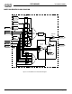
ESS Technology, Inc. C3 . 1 2 X1 HE A DE R 1 2 J1 R2 0 0 S MD P A DS J P1 1 H 2 L 3 V CC 7 4 L S1 3 8 Y0 Y1 Y2 Y3 Y4 Y5 Y6 Y7 9 3 L C6 6 I N T ROM R2 1 10K 15 14 13 12 11 10 9 7 US E 0 o h m R E S I S T O R T O CONNE CT P A DS J P1 L H C5 . 1 D[ 7 . . 0 ] V CC G1 G2 A G2 B A B C U2 10K R1 DOCK E D ohm 6 4 5 A1 2 C4 . 1 1 2 3 V CC V CC A1 5 A1 4 A1 3 PC-SPEAKER-IN AEN NOT E : INSTALL THIS RESISTOR IF T HE 7 4 L S 1 3 8 IS NOT INSTALLED A[ 1 5 . . 0 ] V CC C6 .
SAM0025A-062397 D R QD D R QA IRQD IRQE IRQB IRQC D R QB D R QC IRQA C5 4 10 C5 2 10 VCC D1 D2 D3 D4 D5 D6 D7 D8 D9 D1 D1 D1 D1 D1 D1 D1 D1 D1 B1 B2 B3 B4 B5 B6 B7 B8 B9 B1 B1 B1 B1 B1 B1 B1 B1 B1 B1 B2 B2 B2 B2 B2 B2 B2 B2 B2 B2 B3 B3 0 1 2 3 4 5 6 7 8 0 1 2 3 4 5 6 7 8 9 0 1 2 3 4 5 6 7 8 9 0 1 AT3 6 - ME MC S 1 6 - S B H E SA2 3 -IOCS16 SA2 2 IRQ10 SA2 1 IRQ11 SA2 0 IRQ12 SA1 9 IRQ15 SA1 8 IRQ14 SA1 7 - DACK0 - ME MR D R E Q0 - ME MW - DACK5 SD8 D R E Q5 SD9 - DACK6 SD1 0 D R E Q6 S
ESS Technology, Inc. $ 287 / $ 287 5 3 & 6 3 .2 9''$ 9 & & 5 . 5 . & & 5 . & 5 & . . . 5 5 5 . 5 . 5 . & . 5 & . 5 & 5 . 5 )(55,7( %($' / 8 / 0 & RKP 5 RKP 5 & & & & 6 3 ( $ .
PRELIMINARY ES1879 DATA SHEET APPENDIX D: SCHEMATIC EXAMPLES VCC D2 J 7 XA0 XA1 XA2 XA3 XSC XSD D OC K E D 1 3 5 7 9 1 1 1 1 1 - 12V +12V 1 3 5 7 9 1 1 1 1 1 2 HEADER S1 S W P U S H B U T T ON 1 N4 1 4 8 D3 2 4 6 8 0 2 4 6 8 0 S W P U S H B U T T ON S2 1 N4 1 4 8 V OL U P 1 8 7 8 V OL D N 1 8 7 8 S3 S W P U S H B U T T ON 1 0 X2 J 6 IDATA ISCLK I L R 1 3 5 2 4 6 I2S_INTF_CONN VCC J 5 1 3 5 7 9 1 1 1 1 1 2 2 2 13x 2 1 3 5 7 9 1 3 5 1 1 1 1 1 2 2 2 2 2 4 6 8 0 2 4 6 8 0 2 4 6 HEADER M
PRELIMINARY ES1879 DATA SHEET APPENDIX E: LAYOUT GUIDELINES APPENDIX E: LAYOUT GUIDELINES PCB Layout A grouped on one side of the PCB. Notebook, Motherboard, Pen-based, and PDA portable computers have the following similarity in PCB layout design: B separated on both sides of the PCB. In Case B, audio component grouping will take less space. 6. Multi-layer (usually 4 to 8 layer). Analog Ground Plane 7. Double-sided SMT.
PRELIMINARY ES1879 DATA SHEET APPENDIX F: ES1879 BILL OF MATERIALS APPENDIX F: ES1879 BILL OF MATERIALS Table 36 ES1879 Bill of Materials (BOM) Item Quantity Reference Part 1 2 C1, C2 22 pF 2 15 C3, C4, C5, C6, C7, C8, C12, C14, C40, C41, C44, C45, C50, C53, C55 0.1 µF 3 10 C9, C10, C11, C15, C17, C18, C19, C21, C47, C48 0.22 µF 4 2 C13, C43 47 µF 5 1 C16 0.047 µF 6 10 C20, C26, C27, C28, C29, C30, C31, C32, C38, C39 0.
ES1879 DATA SHEET PRELIMINARY APPENDIX F: ES1879 BILL OF MATERIALS Table 36 ES1879 Bill of Materials (BOM) Item Quantity Reference Part 40 1 U3 78L05 41 1 U5 93LC66 42 1 U7 LM1877 43 1 Y1 14.318 MHz 44 1 JP1 (H = Internal ROM) (L = External EEPROM) 0 ohm Resistor ESS Technology, Inc.
PRELIMINARY ES1879 DATA SHEET APPENDIX F: ES1879 BILL OF MATERIALS No part of this publication may be reproduced, stored in a retrieval system, transmitted, or translated in any form or by any means, electronic, mechanical, manual, optical, or otherwise, without the prior written permission of ESS Technology, Inc. ESS Technology, Inc. makes no representations or warranties regarding the content of this document. All specifications are subject to change without prior notice. (P) U.S.