
Specifications

20 SAM0025A-062397 ESS Technology, Inc.
ES1879 DATA SHEET
PERIPHERAL INTERFACING
PRELIMINARY
I
2
S Serial Interface
Three input pins, IIDATA, IISCLK, and IILR, are used for a
serial interface between an external device and a stereo
DAC within the ES1879. IIDATA, IISCLK, and IILR can be
left floating or connected to ground if the serial interface is
not used.
A typical applications of the I
2
S serial interface is MPEG
audio or CD audio.
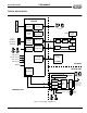
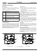
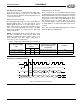
Figure 9 I
2
S Implementation in ES1879
.
I
2
S Serial Interface Software Enable
By hardware reset default, the I
2
S interface is disabled. Bit
6 of Vendor-Defined Card-Level register 29h enables the
I
2
S interface when it is set high. This register is accessed
through the configuration device. In addition, bit 6 of mixer
register 71h enables the data bus connection to the I
2
S
interface. Both these bits must be set in order to enable
the interface.
I
2
S Serial Interface Format Select
The I
2
S serial interface supports two different formats:
ES689/ES69x two-wire serial interface and I
2
S. When
used in the ES689/ES69x format, IIDATA is the serial data
and IISCLK is the bit clock. The IILR input is not used and
can be left floating or connected to ground. Vendor-
Defined Card-Level register 29h bits 5 and 4 select the
format (this register is accessed through the configuration
device). See Vendor-Defined Card-Level register 29h
under “PnP Configuration and Registers” on page 30 for
more detailed information.
I
2
S Serial Interface Timing
This section discusses the I
2
S serial interface signals. The
signals when the port is configured for use with an ES689/
ES69x wavetable synthesizer are defined in the
Wavetable Interface section.
Three signals (plus one optional) are used for I
2
S:
IISCLK The shift clock. The maximum rate is 6.4 MHz.
The minimum number of IISCLK periods per
IILR period is 32. Any number greater than or
equal to 32 is acceptable.
IILR Sample synchronization signal. The maximum
sample rate is 50 kHz.
IIDATA Serial data.
Within the ES1879, IILR and IIDATA are sampled on the
rising edge of IISCLK. See Figure 25 and Figure 26 for
detailed I
2
S timing.
Wavetable Interface
The ES1879 contains a synchronous serial interface for
connection to a wavetable music synthesizer.
MPU-401 Interface
The MPU-401 port can be used for interfacing with MIDI.
MIDI
The ES1879 has an MPU-401 MIDI interface with a 23-
byte receive FIFO and an 8-byte transmit FIFO. The
output of the transmit FIFO is serialized out the MSO pin
and also sent to the ES978 in the expansion unit, where
it is serialized out the MSO pin of that chip.
MIDI data can be received from either the MSI pin of the
ES1879 or from the MSI pin of the ES978 in the expansion
unit. In the unlikely event that MIDI data is received from
both sources simultaneously, the data might be corrupted.
Data received by the ES978 is transmitted back to the
ES1879 in the next upload frame and then placed in the
MPU-401 receive FIFO.
Table 5 I
2
S Interface Pins
Pin Description
IIDATA
Serial data for I
2
S interface. This pin has an inter-
nal pull-down to GNDD.
IISCLK
Serial shift clock for I
2
S interface. This pin has an
internal pull-down to GNDD.
IILR
Left/Right signal for I
2
S interface. This pin has an
internal pull-down to GNDD.
PC CARD
IIDATA
IISCLK
IILR
ES1879
Table 6 Wavetable Interface Pins
Pin Description
MCLK Serial clock from external ES689/ES69x music
synthesizer (2.75 MHz). Input with pull-down.
MSD Serial data from external ES689/ES69x music
synthesizer. When both MCLK and MSD are
active, the stereo DACs normally used by the FM
synthesizer are acquired for use by the external
ES689/ES69x. The normal FM output is blocked.
Input with pull-down.