
User's Manual

8
www.lairdtech.com
Laird Technologies
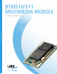
BTM510/511
Bluetooth
®
Multimedia Module
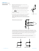
NOTES FOR PCB LAYOUT:
1. The RF output pin must be matched to a 50Ω strip-line or coplanar waveguide on the antenna-less version (BTM510).
2. Ensure that there are no exposed conductors under the module to avoid shorts to the test points on the module underside.
3. ThePCBfootprintisprovidedforguidanceonly.UsersmaywishtomodifythePCBlanddimensionstosuittheirspecic
manufacturing or process.
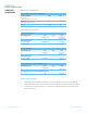
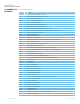
OPERATING PARAMETERS
RECOMMENDED OPERATING CONDITIONS
Operating Condition Min Max
VDD_USB
(USB compatibility not required)
1.7 3.6
VDD_USB
(USB compatibility required)
3.1 3.6
VDD_IO 1.7 3.3
VDD_IN 3.0 3.6
VOLTAGE SPECIFICATIONS
LOGIC LEVELS (VUSB)
Input Voltage Levels Min Typ Max
V
ih
0.625VDD_USB VDD_USB+0.3
V
il
-0.3 0.25VDD_USB
Output Voltage Levels
V
oh
(Iout = -4mA) 0.75VDD_USB VDD_USB
V
ol
(Iout = 4mA) 0 0.125
LOGIC LEVELS (VIO)
Input Voltage Levels Min Typ Max
V
ih
0.625VDD_IO VDD_IO+0.3
V
il
-0.3 0.25VDD_IO
Output Voltage Levels
V
oh
(Iout = -4mA) 0.75VDD_IO VDD_IO
V
ol
(Iout = 4mA) 0 0.125
LOGIC LEVELS (VUSB – USB TERMINALS D+, D-)
Input Voltage Levels Min Typ Max
V
ih
0.7VDD_USB
V
il
0.3VDD_USB
Output Voltage Levels (to correctly terminated USB cable)
V
oh
2.8 VDD_USB
V
ol
0 0.2
OPERATING
PARAMETERS