
Datasheet


©1993 Fairchild Semiconductor Corporation www.fairchildsemi.com
74VHC125 Rev. 1.4.0 3
74VHC125 — Quad Buffer with 3-STATE Outputs
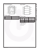
Absolute Maximum Ratings
Stresses exceeding the absolute maximum ratings may damage the device. The device may not function or be
operable above the recommended operating conditions and stressing the parts to these levels is not recommended.
In addition, extended exposure to stresses above the recommended operating conditions may affect device reliability.
The absolute maximum ratings are stress ratings only.
Recommended Operating Conditions
(1)
The Recommended Operating Conditions table defines the conditions for actual device operation. Recommended
operating conditions are specified to ensure optimal performance to the datasheet specifications. Fairchild does not
recommend exceeding them or designing to absolute maximum ratings.
Note:
1. Unused inputs must be held HIGH or LOW. They may not float.
Symbol Parameter Rating
V
CC
Supply Voltage –0.5V to +7.0V
V
IN
DC Input Voltage –0.5V to +7.0V
V
OUT
DC Output Voltage –0.5V to V
CC
+ 0.5V
I
IK
Input Diode Current –20mA
I
OK
Output Diode Current ±20mA
I
OUT
DC Output Current ±25mA
I
CC
DC V
CC
/ GND Current ±50mA
T
STG
Storage Temperature –65°C to +150°C
T
L
Lead Temperature (Soldering, 10 seconds) 260°C
Symbol Parameter Rating
V
CC
Supply Voltage 2.0V to +5.5V
V
IN
Input Voltage 0V to +5.5V
V
OUT
Output Voltage 0V to V
CC
T
OPR
Operating Temperature –40°C to +85°C
t
r
, t
f
Input Rise and Fall Time,
V
CC
=
3.3V ± 0.3V
V
CC
=
5.0V ± 0.5V
0ns/V
∼
100ns/V
0ns/V
∼
20ns/V