
Datasheet

©2006 Fairchild Semiconductor Corporation www.fairchildsemi.com
CNY17XM, CNY17FXM, MOC810XM Rev. 1.1.1 2
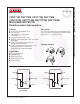
CNY17XM, CNY17FXM, MOC810XM — Phototransistor Optocouplers
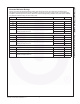
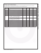
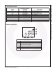
Absolute Maximum Ratings
Stresses exceeding the absolute maximum ratings may damage the device. The device may not function or be
operable above the recommended operating conditions and stressing the parts to these levels is not recommended.
In addition, extended exposure to stresses above the recommended operating conditions may affect device reliability.
The absolute maximum ratings are stress ratings only.
Symbol Parameters Value Units
TOTAL DEVICE
T
STG
Storage Temperature -40 to +150 °C
T
OPR
Operating Temperature -40 to +100 °C
T
J
Junction Temperature -40 to +125 ºC
T
SOL
Lead Solder Temperature 260 for 10 sec °C
P
D
Total Device Power Dissipation @ 25°C (LED plus detector)
Derate Linearly From 25°C
250 mW
2.94 mW/°C
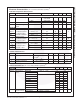
EMITTER
I
F
Continuous Forward Current 60 mA
V
R
Reverse Voltage 6 V
I
F
(pk) Forward Current – Peak (1µs pulse, 300pps) 1.5 A
P
D
LED Power Dissipation 25°C Ambient
Derate Linearly From 25°C
120 mW
1.41 mW/°C
DETECTOR
I
C
Continuous Collector Current 50 mA
V
CEO
Collector-Emitter Voltage 70 V
V
ECO
Emitter Collector Voltage 7 V
P
D
Detector Power Dissipation @ 25°C
Derate Linearly from 25°C
150 mW
1.76 mW/°C