
Datasheet


October 2009
2009 Fairchild Semiconductor Corporation
FDC2512 Rev B4 (W)
FDC2512
150V N-Channel PowerTrench
MOSFET
General Description
This N-Channel MOSFET has been designed
specifically to improve the overall efficiency of DC/DC
converters using either synchronous or conventional
switching PWM controllers. It has been optimized for
low gate charge, low R
DS(ON)
and fast switching speed.
Applications
• DC/DC converter
Features
• 1.4 A, 150 V. R
DS(ON)
= 425 mΩ @ V
GS
= 10 V
R
DS(ON)
= 475 mΩ @ V
GS
= 6 V
• High performance trench technology for extremely
low R
DS(ON)
• Low gate charge (8nC typ)
• High power and current handling capability
• Fast switching speed
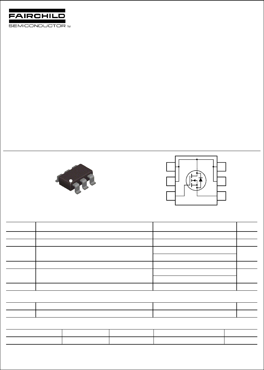
D
D
D
S
D
G
SuperSOT -6
TM
6
5
4
1
2
3
Absolute Maximum Ratings T
A
=25
o
C unless otherwise noted
Symbol Parameter Ratings Units
V
DSS
Drain-Source Voltage 150 V
V
GSS
Gate-Source Voltage
± 20
V
I
D
Drain Current – Continuous (Note 1a) 1.4
A
– Pulsed 8
Maximum Power Dissipation (Note 1a) 1.6 W P
D
(Note 1b)
0.8
T
J
, T
stg
Operating and Storage Junction Temperature Range
−55 to +150 °C
Thermal Characteristics
R
θJA
Thermal Resistance, Junction-to-Ambient
(Note 1a) 78
°C/W
R
θJC
Thermal Resistance, Junction-to-Case
(Note 1) 30
°C/W
Package Marking and Ordering Information
Device Marking Device Reel Size Tape width Quantity
.252 FDC2512 7’’ 8mm 3000 units
FDC2512
E
AS
Single Pulse Avalanche Energy
13.5 mJ
(Note 3)