
Datasheet

FDD5614P Rev C1(W)
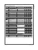
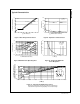
Notes:
1. R
θJA
is the sum of the junction-to-case and case-to-ambient thermal resistance where the case thermal reference is defined as the solder mounting surface of
the drain pins. R
θJC
is guaranteed by design while R
θCA
is determined by the user's board design.
a) R
θJA
= 40°C/W when mounted on a
1in
2
pad of 2 oz copper
b) R
θJA
= 96°C/W when mounted
on a minimum pad.
Scale 1 : 1 on letter size paper
2. Pulse Test: Pulse Width < 300µs, Duty Cycle < 2.0%
3. Maximum current is calculated as:
where P
D
is maximum power dissipation at T
C
= 25°C and R
DS(on)
is at T
J(max)
and V
GS
= 10V. Package current limitation is 21A
)ON(DS
D
R
P
FDD5614P