
Datasheet


July 2005
2005 Fairchild Semiconductor Corp.
FDD6670A Rev E1(W)
FDD6670A
30V N-Channel PowerTrench
MOSFET
General Description
This N-Channel MOSFET has been designed
specifically to improve the overall efficiency of DC/DC
converters using either synchronous or conventional
switching PWM controllers. It has been optimized for
low gate charge, low RDS ( ON) , fast switching speed and
extremely low R
DS(ON)
in a small package.
Applications
• DC/DC converter
• Motor Drives
Features
• 66 A, 30 V R
DS(ON)
= 8 mΩ @ V
GS
= 10 V
R
DS(ON)
= 10 mΩ @ V
GS
= 4.5 V
• Low gate charge
• Fast Switching
• High performance trench technology for extremely
low R
DS(ON)
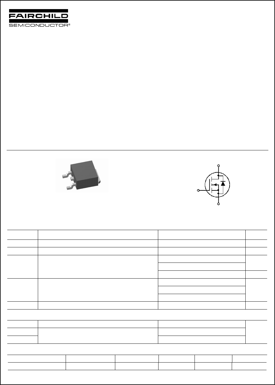
G
S
D
TO-252
D-PAK
(TO-252)
S
G
D
Absolute Maximum Ratings T
A
=25
o
C unless otherwise noted
Symbol Parameter Ratings Units
V
DSS
Drain-Source Voltage 30 V
V
GSS
Gate-Source Voltage
±20
V
I
D
Continuous Drain Current @T
C
=25°C (Note 3) 66 A
@T
A
=25°C (Note 1a) 15
Pulsed (Note 1a) 100
Power Dissipation @T
C
=25°C (Note 3) 63
@T
A
=25°C (Note 1a) 3.2
P
D
@T
A
=25°C (Note 1b) 1.3
W
T
J
, T
STG
Operating and Storage Junction Temperature Range –55 to +175
°C
Thermal Characteristics
R
θJC
Thermal Resistance, Junction-to-Case (Note 1) 2.4 °C/W
R
θJA
Thermal Resistance, Junction-to-Ambient (Note 1a) 40
R
θJA
(Note 1b)
96
Package Marking and Ordering Information
Device Marking Device Package Reel Size Tape width Quantity
FDD6670A FDD6670A D-PAK (TO-252) 13’’ 12mm 2500 units
FDD6670A