
Datasheet

December 2001
2001 Fairchild Semiconductor Corporation
FDG6316P Rev D W)
FDG6316P
P-Channel 1.8V Specified PowerTrench
MOSFET
General Description
This P-Channel 1.8V specified MOSFET uses
Fairchild’s advanced low voltage PowerTrench process.
It has been optimized for battery power management
applications.
Applications
• Battery management
• Load switch
Features
• –0.7 A, –12 V. R
DS(ON)
= 270 mΩ @ V
GS
= –4.5 V
R
DS(ON)
= 360 mΩ @ V
GS
= –2.5 V
R
DS(ON)
= 650 mΩ @ V
GS
= –1.8 V
• Low gate charge
• High performance trench technology for extremely
low R
DS(ON)
• Compact industry standard SC70-6 surface mount
package
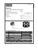
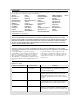
S
G
D
D
G
S
Pin 1
SC70-6
S
G
D
D
G
S
6 or 3
5 or 2
4 or 1
1 or 4
2 or 5
3 or 6
The pinouts are symmetrical; pin 1 and pin 4 are interchangeable.
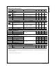
Absolute Maximum Ratings T
A
=25
o
C unless otherwise noted
Symbol Parameter Ratings Units
V
DSS
Drain-Source Voltage –12 V
V
GSS
Gate-Source Voltage
± 8
V
I
D
Drain Current – Continuous (Note 1) –0.7 A
– Pulsed –1.8
P
D
Power Dissipation for Single Operation (Note 1) 0.3 W
T
J
, T
STG
Operating and Storage Junction Temperature Range –55 to +150
°C
Thermal Characteristics
R
θJA
Thermal Resistance, Junction-to-Ambient
(Note 1) 415
°C/W
Package Marking and Ordering Information
Device Marking Device Reel Size Tape width Quantity
.16 FDG6316P 7’’ 8mm 3000 units
FDG6316P