
Datasheet

FDG6316P Rev D (W)
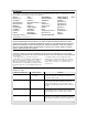
Electrical Characteristics T
A
= 25°C unless otherwise noted
Symbol Parameter Test Conditions Min Typ Max Units
Off Characteristics
BV
DSS
Drain–Source Breakdown
Voltage
V
GS
= 0 V, I
D
= –250 µA
–12 V
∆BVDSS
∆T
J
Breakdown Voltage Temperature
Coefficient
I
D
= –250 µA, Referenced to 25°C
–3.7
mV/°C
I
DSS
Zero Gate Voltage Drain Current V
DS
= –10 V, V
GS
= 0 V –1
µA
I
GSSF
Gate–Body Leakage, Forward V
GS
= –8 V, V
DS
= 0 V –100 nA
I
GSSR
Gate–Body Leakage, Reverse V
GS
= 8 V, V
DS
= 0 V 100 nA
On Characteristics (Note 2)
V
GS(th)
Gate Threshold Voltage
V
DS
= V
GS
, I
D
= –250 µA
–0.4 –0.6 –1.5 V
∆VGS(th)
∆T
J
Gate Threshold Voltage
Temperature Coefficient
I
D
= –250 µA, Referenced to 25°C
2
mV/°C
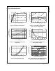
R
DS(on)
Static Drain–Source
On–Resistance
V
GS
= –4.5 V, I
D
= –0.7 A
V
GS
= –2.5 V, I
D
= –0.5 A
V
GS
= –1.8 V, I
D
= –0.4 A
V
GS
= –4.5 V, I
D
= –0.7 A, T
J
=125°C
221
297
427
250
270
360
650
348
mΩ
I
D(on)
On–State Drain Current V
GS
= –4.5 V, V
DS
= –5 V –1.8 A
g
FS
Forward Transconductance V
DS
= –5 V, I
D
= –0.7 A 2.5 S
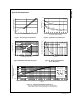
Dynamic Characteristics
C
iss
Input Capacitance 146 pF
C
oss
Output Capacitance 60 pF
C
rss
Reverse Transfer Capacitance
V
DS
= –6 V, V
GS
= 0 V,
f = 1.0 MHz
48 pF
Switching Characteristics (Note 2)
t
d(on)
Turn–On Delay Time 5 10 ns
t
r
Turn–On Rise Time 13 23 ns
t
d(off)
Turn–Off Delay Time 8 16 ns
t
f
Turn–Off Fall Time
V
DD
= –6 V, I
D
= 1 A,
V
GS
= –4.5 V, R
GEN
= 6 Ω
2 4 ns
Q
g
Total Gate Charge 1.7 2.4 nC
Q
gs
Gate–Source Charge 0.3 nC
Q
gd
Gate–Drain Charge
V
DS
= –6 V, I
D
= –0.7 A,
V
GS
= –4.5 V
0.4 nC
Drain–Source Diode Characteristics and Maximum Ratings
I
S
Maximum Continuous Drain–Source Diode Forward Current –0.25 A
V
SD
Drain–Source Diode Forward
Voltage
V
GS
= 0 V, I
S
= –0.25 A(Note 2) –0.7 –1.2 V
Notes:
1. R
θJA
is the sum of the junction-to-case and case-to-ambient thermal resistance where the case thermal reference is defined as the solder mounting surface of
the drain pins. R
θJC
is guaranteed by design while R
θJA
is determined by the user's board design. R
θJA
= 415°C/W when mounted on a minimum pad of FR-4
PCB on still air environment
2. Pulse Test: Pulse Width < 300µs, Duty Cycle < 2.0%
FDG6316P