
Datasheet


June 2014
FDMC2523P P-Channel QFET
®
©2012 Fairchild Semiconductor Corporation
FDMC2523P Rev.C6
www.fairchildsemi.com
1
FDMC2523P
P-Channel QFET
®
-150V, -3A, 1.5Ω
Features
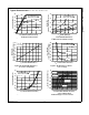
Max r
DS(on)
= 1.5Ω at V
GS
= -10V, I
D
= -1.5A
Low Crss ( typical 10pF)
Fast Switching
Low gate charge ( typical 6.2 nC )
Improved dv / dt capability
RoHS Compliant
General Description
These P-Channel MOSFET enhancement mode power field
effect transistors are produced using Fairchild's proprietary,
planar stripe, DMOS technology. This advanced technology has
been especially tailored to minimize on-state resistance, provide
superior switching performance, and withstand high energy
pulse in the avalanche and commutation mode. These devices
are well suited for low voltage applications such as audio
amplifier, high efficiency switching DC/DC converters, and DC
motor control.
Application
Active Clamp Switch
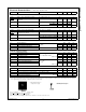
MOSFET Maximum Ratings T
A
= 25°C unless otherwise noted
Thermal Characteristics
Package Marking and Ordering Information
Symbol Parameter Ratings Units
V
DS
Drain to Source Voltage -150 V
V
GS
Gate to Source Voltage ±30 V
I
D
Drain Current -Continuous T
C
= 25°C -3
A -Continuous T
C
= 100°C -1.8
-Pulsed -12
P
D
Power Dissipation (Steady State) T
C
= 25°C 42 W
E
AS
Single Pulse Avalanche Energy (Note 5) 3.3 mJ
T
J
, T
STG
Operating and Storage Junction Temperature Range -55 to +150 °C
T
L
Maximum lead temperature for soldering purposes, 1/8” from case for 5 seconds 300 °C
dv/dt Peak Diode Recovery dv/dt (Note 2) -5 V/ns
R
θJC
Thermal Resistance, Junction to Case (Note 1) 3.0
°C/W
R
θJA
Thermal Resistance, Junction to Ambient (Note 1a) 60
Device Marking Device Package Reel Size Tape Width Quantity
2523P FDMC2523P MLP 3.3x3.3 13 ’’ 12 mm 3000 units
Bottom
D
D
D
D
S
S
S
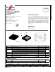
G
Top
Pin 1
MLP 3.3x3.3
S
S
S
G
D
D
D
D