
Datasheet

www.fairchildsemi.com
2
©2011 Fairchild Semiconductor Corporation
FDMC8015L Rev. C1
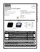
FDMC8015L N-Channel PowerTrench
®
MOSFET
TM
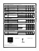
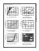
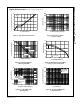
Electrical Characteristics T
J
= 25 °C unless otherwise noted
Off Characteristics
On Characteristics
Dynamic Characteristics
Switching Characteristics
Drain-Source Diode Characteristics
Symbol Parameter Test Conditions Min Typ Max Units
BV
DSS
Drain to Source Breakdown Voltage I
D
= 250 μA, V
GS
= 0 V 40 V
ΔBV
DSS
ΔT
J
Breakdown Voltage Temperature
Coefficient
I
D
= 250 μA, referenced to 25 °C 36 mV/°C
I
DSS
Zero Gate Voltage Drain Current V
DS
= 32 V, V
GS
= 0 V 1 μA
I
GSS
Gate to Source Leakage Current V
GS
= ±20 V, V
DS
= 0 V ±100 nA
V
GS(th)
Gate to Source Threshold Voltage V
GS
= V
DS
, I
D
= 250 μA11.83V
ΔV
GS(th)
ΔT
J
Gate to Source Threshold Voltage
Temperature Coefficient
I
D
= 250 μA, referenced to 25 °C -6 mV/°C
r
DS(on)
Static Drain to Source On Resistance
V
GS
= 10 V, I
D
= 7 A 19.7 26
mΩV
GS
= 4.5 V, I
D
= 6 A 24 36
V
GS
= 10 V, I
D
= 7 A, T
J
= 125 °C 29 39
g
FS
Forward Transconductance V
DD
= 5 V, I
D
= 7 A 30 S
C
iss
Input Capacitance
V
DS
= 20 V, V
GS
= 0 V,
f = 1 MHz
710 945 pF
C
oss
Output Capacitance 94 125 pF
C
rss
Reverse Transfer Capacitance 58 90 pF
R
g
Gate Resistance 1.2 Ω
t
d(on)
Turn-On Delay Time
V
DD
= 20 V, I
D
= 7 A,
V
GS
= 10 V, R
GEN
= 6 Ω
6.3 13 ns
t
r
Rise Time 1.9 10 ns
t
d(off)
Turn-Off Delay Time 18 33 ns
t
f
Fall Time 1.7 10 ns
Q
g(TOT)
Total Gate Charge V
GS
= 0 V to 10 V
V
DD
= 20 V,
I
D
= 7 A
13.6 19 nC
Q
g(TOT)
Total Gate Charge V
GS
= 0 V to 4.5 V 6.6 10 nC
Q
gs
Total Gate Charge 1.9 nC
Q
gd
Gate to Drain “Miller” Charge 2.5 nC
V
SD
Source to Drain Diode Forward Voltage
V
GS
= 0 V, I
S
= 7 A (Note 2) 0.84 1.2
V
V
GS
= 0 V, I
S
= 2 A (Note 2) 0.76 1.1
t
rr
Reverse Recovery Time
I
F
= 7 A, di/dt = 100 A/μs
18 33 ns
Q
rr
Reverse Recovery Charge 8.6 18 nC
NOTES:
1. R
θJA
is determined with the device mounted on a 1 in
2
pad 2 oz copper pad on a 1.5 x 1.5 in. board of FR-4 material. R
θJC
is guaranteed by design while R
θCA
is determined by
the user's board design.
2. Pulse Test: Pulse Width < 300 μs, Duty cycle < 2.0%.
3. Starting T
J
= 25 °C; N-ch: L = 1 mH, I
AS
= 8 A, V
DD
= 36 V, V
GS
= 10 V.
53 °C/W when mounted on a
1 in
2
pad of 2 oz copper
125 °C/W when mounted on
a minimum pad of 2 oz copper
a.
b.