
Datasheet

FDMS7672AS N-Channel PowerTrench
®
SyncFET
TM
©2009 Fairchild Semiconductor Corporation
FDMS7672AS Rev.C
www.fairchildsemi.com
1
September 2009
FDMS7672AS
N-Channel PowerTrench
®
SyncFET
TM
30 V, 42 A, 4 mΩ
Features
Max r
DS(on)
= 4.0 mΩ at V
GS
= 10 V, I
D
= 18 A
Max r
DS(on)
= 4.5 mΩ at V
GS
= 7 V, I
D
= 16 A
Advanced Package and Silicon combination for low r
DS(on)
and high efficiency
SyncFET Schottky Body Diode
MSL1 robust package design
100% UIL tested
RoHS Compliant
General Description
The FDMS7672AS has been designed to minimize losses in
power conversion application. Advancements in both silicon and
package technologies have been combined to offer the lowest
r
DS(on)
while maintaining excellent switching performance. This
device has the added benefit of an efficient monolithic Schottky
body diode.
Applications
Synchronous Rectifier for DC/DC Converters
Notebook Vcore/ GPU low side switch
Networking Point of Load low side switch
Telecom secondary side rectification
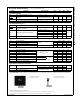
MOSFET Maximum Ratings T
A
= 25 °C unless otherwise noted
Thermal Characteristics
Package Marking and Ordering Information
Symbol Parameter Ratings Units
V
DS
Drain to Source Voltage 30 V
V
GS
Gate to Source Voltage (Note 4) ±20 V
I
D
Drain Current -Continuous (Package limited) T
C
= 25 °C 42
A
-Continuous (Silicon limited) T
C
= 25 °C 83
-Continuous T
A
= 25 °C (Note 1a) 19
-Pulsed 90
dv/dt MOSFET dv/dt 2.6 V/ns
E
AS
Single Pulse Avalanche Energy (Note 3) 60 mJ
P
D
Power Dissipation T
C
= 25 °C 46
W
Power Dissipation T
A
= 25 °C (Note 1a) 2.5
T
J
, T
STG
Operating and Storage Junction Temperature Range -55 to +150 °C
R
θJC
Thermal Resistance, Junction to Case 2.7
°C/W
R
θJA
Thermal Resistance, Junction to Ambient (Note 1a) 50
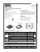
Device Marking Device Package Reel Size Tape Width Quantity
FDMS7672AS FDMS7672AS Power 56 13 ’’ 12 mm 3000 units
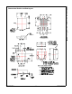
4
3
2
1
5
6
7
8
Power 56
D
D
D
D
S
S
S
G
D
D
D
D
G
S
S
S
Pin 1
Bottom
Top