
Datasheet


December 2010
©2010 Fairchild Semiconductor Corporation
FDMS86103L Rev.C
www.fairchildsemi.com
1
FDMS86103L N-Channel Power Trench
®
MOSFET
FDMS86103L
N-Channel PowerTrench
®
MOSFET
100 V, 49 A, 8 mΩ
Features
Max r
DS(on)
= 8 mΩ at V
GS
= 10 V, I
D
= 12 A
Max r
DS(on)
= 11 mΩ at V
GS
= 4.5 V, I
D
= 10 A
Advanced Package and Silicon combination for low r
DS(on)
and high efficiency
MSL1 robust package design
100% UIL tested
RoHS Compliant
General Description
This N-Channel MOSFET is produced using Fairchild
Semiconductor‘s advanced Power Trench
®
process thant has
been especially tailored to minimize the on-state resistance and
yet maintain superior switching performance.
Application
DC-DC Conversion
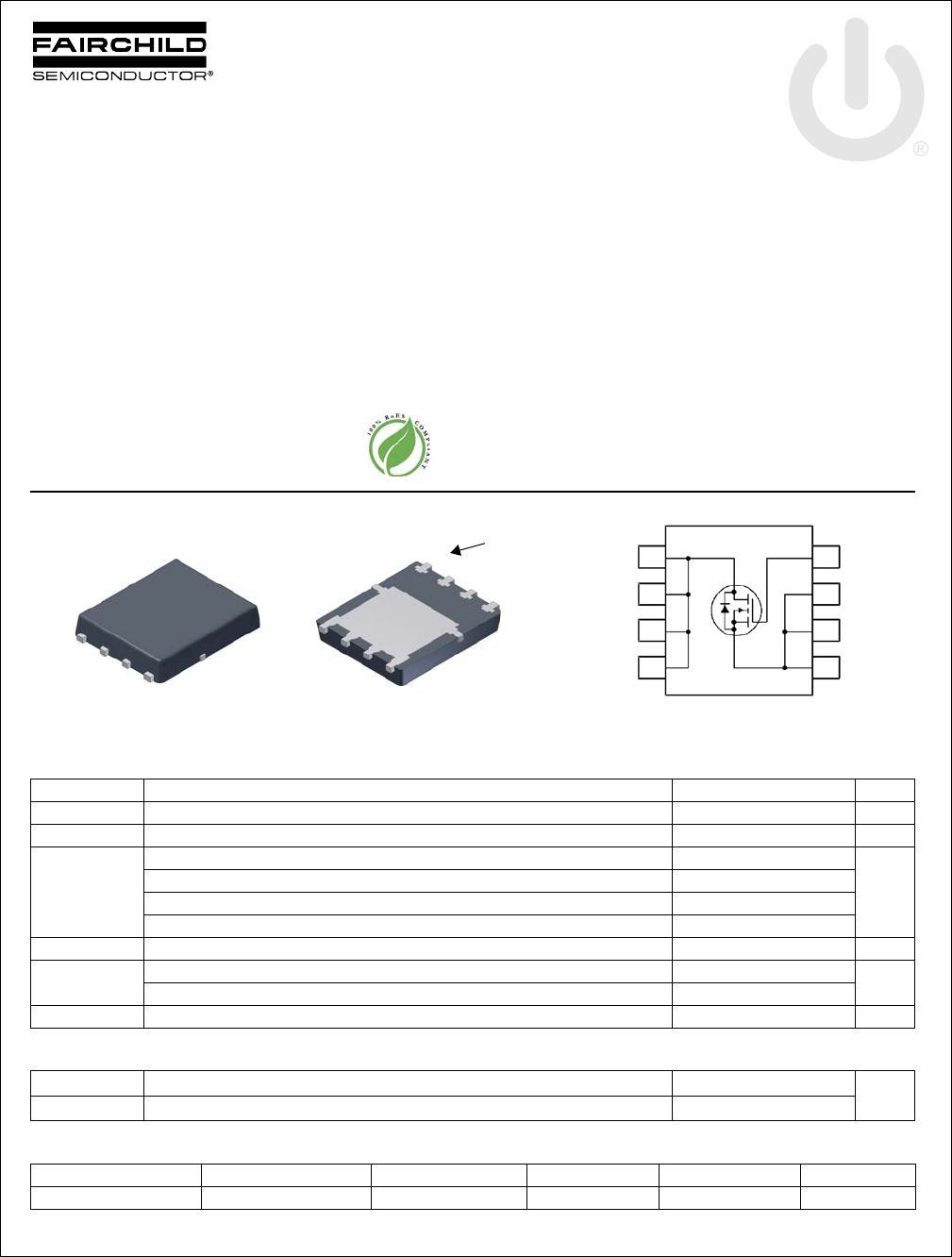
G
S
S
S
D
D
D
D
5
6
7
8
3
2
1
4
Bottom
Power 56
Top
Pin 1
G
S
S
S
D
D
D
D
MOSFET Maximum Ratings T
A
= 25 °C unless otherwise noted
Thermal Characteristics
Package Marking and Ordering Information
Symbol Parameter Ratings Units
V
DS
Drain to Source Voltage 100 V
V
GS
Gate to Source Voltage ±20 V
I
D
Drain Current -Continuous (Package limited) T
C
= 25 °C 49
A
-Continuous (Silicon limited) T
C
= 25 °C 81
-Continuous T
A
= 25 °C (Note 1a) 12
-Pulsed 100
E
AS
Single Pulse Avalanche Energy (Note 3) 312 mJ
P
D
Power Dissipation T
C
= 25 °C 104
W
Power Dissipation T
A
= 25 °C (Note 1a) 2.5
T
J
, T
STG
Operating and Storage Junction Temperature Range -55 to +150 °C
R
θJC
Thermal Resistance, Junction to Case 1.2
°C/W
R
θJA
Thermal Resistance, Junction to Ambient (Note 1a) 50
Device Marking Device Package Reel Size Tape Width Quantity
FDMS86103L FDMS86103L Power 56 13 ’’ 12 mm 3000 units