
Datasheet


©2007 Fairchild Semiconductor Corporation 1 www.fairchildsemi.com
FDP33N25 / FDPF33N25T Rev. B
FDP33N25 / FDPF33N25T 250V N-Channel MOSFET
October
UniFET
TM
FDP33N25 / FDPF33N25T
250V N-Channel MOSFET
Features
• 33A, 250V, R
DS(on)
= 0.094Ω @V
GS
= 10 V
• Low gate charge ( typical 36.8 nC)
• Low Crss ( typical 39 pF)
•Fast switching
• Improved dv/dt capability
Description
These N-Channel enhancement mode power field effect
transistors are produced using Fairchild’s proprietary, planar
stripe, DMOS technology.
This advanced technology has been especially tailored to
minimize on-state resistance, provide superior switching
performance, and withstand high energy pulse in the avalanche
and commutation mode. These devices are well suited for high
efficient switched mode power supplies and active power factor
correction.
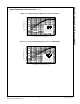
TO-220
FDP Series
G
S
D
TO-220F
FDPF Series
G
S
D
D
G
S
Absolute Maximum Ratings
Symbol Parameter FDP33N25 FDPF33N25T Unit
V
DSS
Drain-Source Voltage 250 V
I
D
Drain Current - Continuous (T
C
= 25°C)
- Continuous (T
C
= 100°C)
33
20.4
33*
20.4*
A
A
I
DM
Drain Current - Pulsed
(Note 1)
132 132*
A
V
GSS
Gate-Source voltage ± 30 V
E
AS
Single Pulsed Avalanche Energy
(Note 2)
918 mJ
I
AR
Avalanche Current
(Note 1)
33 A
E
AR
Repetitive Avalanche Energy
(Note 1)
23.5 mJ
dv/dt Peak Diode Recovery dv/dt
(Note 3)
4.5 V/ns
P
D
Power Dissipation (T
C
= 25°C)
- Derate above 25°C
235
1.89
37
0.29
W
W/°C
T
J,
T
STG
Operating and Storage Temperature Range -55 to +150 °C
T
L
Maximum Lead Temperature for Soldering Purpose,
1/8” from Case for 5 Seconds
300 °C
*Drain current limited by maximum junction temperature
Thermal Characteristics
Symbol Parameter FDP33N25 FDPF33N25T Unit
R
θJC
Thermal Resistance, Junction-to-Case 0.53 3.4 °C/W
R
θCS
Thermal Resistance, Case-to-Sink Typ. 0.5 -- °C/W
R
θJA
Thermal Resistance, Junction-to-Ambient 62.5 62.5 °C/W