
Datasheet


FDS3580
FDS3580 Rev. C
FDS3580
80V N-Channel PowerTrench
MOSFET
December 2000
2000 Fairchild Semiconductor International
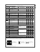
Absolute Maximum Ratings
T
A
= 25°C unless otherwise noted
Symbol Parameter Ratings Units
V
DSS
Drain-Source Voltage 80 V
V
GSS
Gate-Source Voltage
±
20
V
I
D
Drain Current - Continuous
(Note 1a)
7.6 A
- Pulsed 50
P
D
Power Dissipation for Single Operation
(Note 1a)
2.5 W
(Note 1b)
1.2
(Note 1c)
1
T
J
, T
stg
Operating and Storage Junction Temperature Range -55 to +150
°
C
Thermal Characteristics
R
θ
JA
Thermal Resistance, Junction-to-Ambient
(Note 1a)
50
°
C/W
R
θ
JC
Thermal Resistance, Junction-to-Case
(Note 1)
25
°
C/W
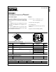
Package Outlines and Ordering Information
Device Marking Device Reel Size Tape Width Quantity
FDS3580 FDS3580 13’’ 12mm 2500 units
6
7
8
5
3
2
1
4
S
D
S
S
SO-8
D
D
D
G
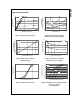
General Description
This N-Channel MOSFET has been designed specifically
to improve the overall efficiency of DC/DC converters using
either synchronous or conventional switching PWM
controllers.
These MOSFETs feature faster switching and lower gate
charge than other MOSFETs with comparable R
DS(ON)
specifications.
The result is a MOSFET that is easy and safer to drive
(even at very high frequencies), and DC/DC power supply
designs with higher overall efficiency.
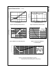
Features
• 7.6 A, 80 V. R
DS(ON
)
= 0.029 Ω @ V
GS
= 10 V
R
DS(ON)
= 0.033 Ω @ V
GS
= 6 V.
• Low gate charge (34nC typical).
• Fast switching speed.
• High performance trench technology for extremely
low R
DS(ON)
.
• High power and current handling capability.