
Datasheet
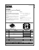


FDS3580
FDS3580 Rev. C
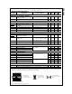
Electrical Characteristics
T
A
= 25°C unless otherwise noted
S
y
mbol Parameter Test Conditions Min T
yp
Max Units
Drain-Source Avalanche Ratings
(Note 2)
W
DSS
Single Pulse Drain-Source
Avalanche Energy
V
DD
= 40 V, I
D
= 7.6 A 245 mJ
I
AR
Maximum Drain-Source Avalanche Current 7.6 A
Off Characteristics
BV
DSS
Drain-Source Breakdown Voltage
V
GS
= 0 V, I
D
= 250
µ
A
80 V
∆
BV
DSS
∆
T
J
Breakdown Voltage Temperature
Coefficient
I
D
= 250
µ
A, Referenced to 25
°
C
81
mV/
°
C
I
DSS
Zero Gate Voltage Drain Current V
DS
= 64 V, V
GS
= 0 V 1
µ
A
I
GSSF
Gate-Body Leakage, Forward V
GS
= 20 V, V
DS
= 0 V 100 nA
I
GSSR
Gate-Body Leakage, Reverse V
GS
= -20 V, V
DS
= 0 V -100 nA
On Characteristics
(Note 2)
V
GS(th)
Gate Threshold Voltage
V
DS
= V
GS
, I
D
= 250
µ
A
22.54 V
∆
V
GS(th)
∆
T
J
Gate Threshold Voltage
Temperature Coefficient
I
D
= 250
µ
A, Referenced to 25
°
C
-7
mV/
°
C
R
DS(on)
Static Drain-Source
On-Resistance
V
GS
= 10 V, I
D
= 7.6 A
V
GS
= 10 V, I
D
= 7.6 A, T
J
=125
°
C
V
GS
= 6 V, I
D
= 7 A
0.022
0.037
0.024
0.029
0.055
0.033
Ω
I
D(on)
On-State Drain Current V
GS
= 10 V, V
DS
= 5 V 30 A
g
FS
Forward Transconductance V
DS
= 5 V, I
D
= 7.6 A 28 S
Dynamic Characteristics
C
iss
Input Capacitance 1800 pF
C
oss
Output Capacitance 180 pF
C
rss
Reverse Transfer Capacitance
V
DS
= 25 V, V
GS
= 0 V,
f = 1.0 MHz
90 pF
Switching Characteristics
(Note 2)
t
d(on)
Turn-On Delay Time 13 26 ns
t
r
Turn-On Rise Time 8 20 ns
t
d(off)
Turn-Off Delay Time 34 60 ns
t
f
Turn-Off Fall Time
V
DD
= 40 V, I
D
= 1 A,
V
GS
= 10 V, R
GEN
= 6
Ω
16 30 ns
Q
g
Total Gate Charge 34 46 nC
Q
gs
Gate-Source Charge 6.1 nC
Q
gd
Gate-Drain Charge
V
DS
= 40 V, I
D
= 7.6 A,
V
GS
= 10 V
6.9 nC
Drain-Source Diode Characteristics and Maximum Ratings
I
S
Maximum Continuous Drain-Source Diode Forward Current 2.1 A
V
SD
Drain-Source Diode Forward Volta
g
eV
GS
= 0 V, I
S
= 2.1 A
(Note 2)
0.74 1.2 V
Notes:
1: R
θJA
is the sum of the junction-to-case and case-to-ambient resistance where the case thermal reference is defined as the solder mounting surface of the
drain pins. R
θJC
is guaranteed by design while R
θCA
is determined by the user's board design.
Scale 1 : 1 on letter size paper
2: Pulse Test: Pulse Width ≤ 300 µs, Duty Cycle ≤ 2.0%
a) 50° C/W when
mounted on a 1 in
2
pad of 2 oz. copper.
b) 105° C/W when
mounted on a 0.04 in
2
pad of 2 oz. copper.
c) 125° C/W when
mounted on a minimum
pad.